This thread has been locked.

If you have a related question, please click the "Ask a related question" button in the top right corner. The newly created question will be automatically linked to this question.

LMX2491: RAMP Length error

Part Number: LMX2491

Hello.


LMX2491 CHIP related question.

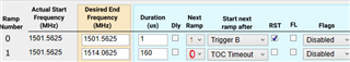
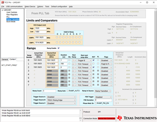
Ramp length is set by register settings.

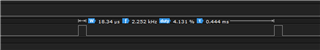
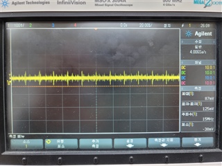
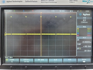
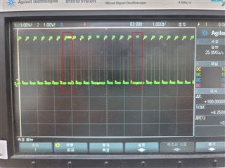
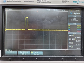
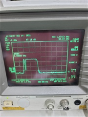
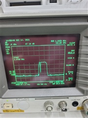
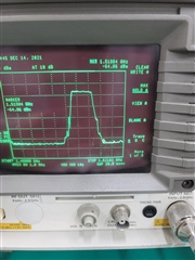
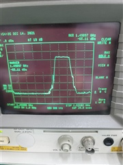
I set a value of 160us, but when I look at the TRIG value, I get 16us.

I don't know why.

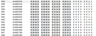
Below is the register setting value.

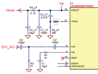
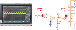
And there is no output to CPOUT either.

So I was wondering if there is something wrong with the register settings.


R106 0x006A04
R105 0x006900
R104 0x006800
R103 0x00673F
R102 0x0066FF
R101 0x0065FA
R100 0x0064E2
R99 0x006343
R98 0x006219
R97 0x006100
R96 0x006000
R95 0x005F00
R94 0x005E03
R93 0x005D33
R92 0x005C34
R91 0x005B00
R90 0x005A28
R89 0x005900
R88 0x005800
R87 0x005700
R86 0x005600
R85 0x005500
R84 0x005400
R83 0x005303
R82 0x005201
R81 0x005100
R80 0x005000
R79 0x004F00
R78 0x004E00
R77 0x004D00
R76 0x004C00
R75 0x004B00
R74 0x004A00
R73 0x004900
R72 0x004800
R71 0x004700
R70 0x004600
R69 0x004500
R68 0x004400
R67 0x0043DA
R66 0x004202
R65 0x004175
R64 0x004000
R63 0x003F00
R62 0x003E8A
R61 0x003D02
R60 0x003C75
R59 0x003B01
R58 0x003A01
R57 0x003900
R45 0x002D00
R44 0x002C00
R43 0x002B00
R42 0x002A00
R41 0x002900
R40 0x002800
R39 0x00273A
R38 0x0026FA
R37 0x0025F2
R36 0x00240F
R35 0x002341
R34 0x002284
R33 0x002120
R32 0x002000
R31 0x001F2A
R30 0x001E06
R29 0x001D00
R28 0x001C1F
R27 0x001B08
R26 0x001A00
R25 0x001901
R24 0x001800
R23 0x001700
R22 0x001600
R21 0x00158A
R20 0x001400
R19 0x001300
R18 0x00122C
R17 0x001100
R16 0x001025
R15 0x000F00
R14 0x000E00
R13 0x000D00
R12 0x000C00
R11 0x000B00
R10 0x000A00
R9 0x000900
R8 0x000800
R7 0x000700
R6 0x000600
R5 0x000500
R4 0x000400
R3 0x000300
R2 0x000201
R1 0x000100
R0 0x000018

  • Hi Kiman,

    If you want a single sawtooth ramp, please follow datasheet section 8.2.5. 

    You only need two ramps to construct the sawtooth waveform. 

    you don't need Ramp Count, please set it to 0.

  • Thanks for the reply first.

    I modified it, but the result is the same.

    For reference, the circuit is as follows.

  • Hi Kiman,

    Can you measure the waveform at CPout pin?

    Another test, simply lock the VCO to 1514.0625 without ramping, does it lock? What is the CPout voltage?

  • Thanks for the reply.

    When measured with an oscilloscope, a signal of about 60~80mv was obtained.

    The signal looked like a fake signal.

    So I asked a question because I thought it had something to do with the part where the length of the lamp did not come out properly.

  • Hi Noel Fung.

    [[Another test, simply lock the VCO to 1514.0625 without ramping, does it lock? What is the CPout voltage?]]

    I would like to proceed with your question.
    But I don't know what to do, so I ask.
    Can you tell me how to set the register and check the operation?

  • Hi Kiman,

    Please try the attached .tcs file.

    After the LMX2491 is powered up and both the reference clock and VCO signal are ready, press Ctrl and L keys to load all the registers to the device. It will lock to 1501.5625MHz and the MUXOUT pin will turn HIGH. Please measure the CPout voltage.

    Then change the VCO frequency to 1514.0625MHz and then press Enter. Again measure the CPout voltage. 

    If the CPout voltages are between 0.5V and 2.8V, and MUXOUT pin is HIGH, we should be able to ramp between these frequencies.

  • .tcs file is here.2491e2e.tcs

  • Thank you for answer.

    I see the Raw Registers value in the TICS PRO program and do spi communication directly from the firmware.

    This is an oscilloscope picture of cpout after spi communication setup.

    As before, a small signal comes out every 16.6us.
    The maximum voltage is between 80 and 100 mv.

  • This is the result of debugging TRIG1 by applying the uploaded tcs file.

    TRIG1 => 5.3us

    It was confirmed that the waveform was generated like this.

  • Hi Kiman,

    If the first plot was taken without ramping at VCO = 1501.5625, then I think the PLL is not locking at all. What was the MUXout pin voltage? I guess it should be LOW.

    let's do some debug.

    Set the MUXout pin to R/4 or N/4. If you see a 10MHz clock with R/4, that means the PLL input path is good, the 40MHz reference clock is ready. If the PLL is locked, you should also see a 10MHz clock with N/4. Since the PLL is not locking right now, you should still see something close. The purpose of these tests is to verify both the input path and feedback path have no issue, the unlock is due to something else.

  • Thank you for answer.

    [[If the first plot was taken without ramping at VCO = 1501.5625, then I think the PLL is not locking at all. What was the MUXout pin voltage? I guess it should be LOW.]]

    => Check that the Low signal is coming out.

    [[Set the MUXout pin to R/4 or N/4. If you see a 10MHz clock with R/4, that means the PLL input path is good, the 40MHz reference clock is ready. If the PLL is locked, you should also see a 10MHz clock with N/4. Since the PLL is not locking right now, you should still see something close. The purpose of these tests is to verify both the input path and feedback path have no issue, the unlock is due to something else.]]

     => When MUXout is set to R/4, 10MHz is obtained, Setting MUXout to N/4 gave me 90 MHz.

  • Hi Kiman,

    OK, there must be something wrong with the VCO signal input. How did you connect the Q1 and Q1N pins of the transceiver to the LMX2491?

  • Thanks for the reply.

    LMX2491 is connected with BGT24LTR22 chip.

    In the case of BGT24LTR22 chip, it is not divided into Q1/Q1N and receives FeedBack with one PIN.

    It is connected to DIV_AO pin of BGT24LTR22 and Fin pin of LMX2491.

    And the same result was obtained even if there was no connection between the DIV_AO pin and the FIN pin.

    I'm not very good at circuit configuration yet, so if there is a problem with the circuit, please let me know.

  • Hi Kiman,

    Fin* pins should not be tied to ground directly.

    Please try below, Fin and Fin* can be swapped, it does not matter which one is the VCO input. The loop filter value is based on a loop bandwidth of 500kHz.

  • Thanks for the reply.

    As shown in the figure below, both the circuit that receives the DIV_AO signal from FIN or the circuit that receives the DIV_AO signal from FIN* can have the same result.

    Either circuit can be used.

  • Hi Kiman

    Yes, both will work.

  • Thanks for the reply.

    After modifying the schematic, I checked the oscilloscope.

    yellow => cpout
    Green => ramp operation section

    If you look at cpout, the waveform shows a different shape in the ramp operation section.

    I wonder if this is correct

    yellow => fin input signal

    And in the case of fin, I checked that about 480mV is maintained, and I wonder if this is normal operation.

  • In addition, the ramp operation was performed periodically.

    Yellow => trig2_mux signal high during ramp operation

    Green => ramp operation cycle

    The ramp operation time was set to 160us.

    However, as seen in the oscilloscope, it took about 370us in one cycle, and it turned out that it did not work in the other cycle.

  • Hi Kiman,

    Let focus on simple PLL operation first, we should do the ramp later once we confirm PLL operation is solid.

    After modifying the schematic, can you make it lock to 1501.5625MHz and 1514.0625MHz? If not, can you get 10MHz from R/4 and N/4? How does the CPout voltage look like? Could you use a spectrum analyzer to check the DIV_AO signal?

  • Thanks for the reply.

    The result of measuring R/4 and N/4 of the previously sent register setting

    R/4 => 10MHz
    N/4 => 7.5~10MHz, one cycle occurs at 100ns~132ns

    In the case of cpout, it is confirmed that it comes out as set between 0 and 2.9v.

    Sorry, spectrum analyzer is not available.

    The value of N/4 seems to be unstable.

  • Hi Kiman,

    So, the VCO is still unlocked, but at least you saw 7.5-10MHz with N/4, we are getting closed. 

    What were the CPout waveform look like at these frequencies?

  • Thanks for the reply.

    The CPOUT signal occurs at random intervals as shown in the figure below.
    And the other picture is an enlarged one of the waveforms.

    If you look at the register settings you sent, all register values between R92 and R86 are set to 0X00. Is this the right setting?

  • Hi Kiman,

    The contents of registers R86 to R92 are empty because I am not going to ramp. 

    What was the VCO frequency in your plots?

    The PLL is not locking at all. We really need a spectrum analyzer to spot the DIV_AO signal, otherwise it would be difficult to debug.

  • Thanks for the reply.

    Spectrum analyzers are difficult to use right now.

    May I know the reason for the lock-in phenomenon?

    Is it usually a circuit configuration issue?

    Usually, if you know which problem is causing the lockout, you want to check that part first.

    The vco frequency uses 24.050 GHz to 24.250 GHz.

  • Hi Kiman,

    We have verified the input path, we could get a stable 10MHz from R/4. The problem is still from the feedback path, we did not get a correct signal from N/4. The signal from CPout is also completely not correct. We have to verify if there is signal with sufficient level going into the Fin pin. This has to be done with a spectrum analyzer. Please try get a spectrum analyzer to verify DIV_AO signal, otherwise I do not have sufficient information to make a guess. 

  • Thanks for the reply.
    I am preparing to check it with a spectrum analyzer.
    Before that, I checked various things with an oscilloscope.
    The FIN connection part is a signal sent from RF, so I checked the RF data sheet again.
    First of all, the power of RF uses 1.5V.
    And if you look at the graph below, the ISM band is between 0.6 and 0.7.
    Even if only ISM BAND frequency is used, is it correct to set the CPM_THR_LOW and CPM_THR_HIGH values as follows?
    CPM_THR_LOW => 0.5V
    CPM_THR_HIGH => 1.5V


    And I checked the position of the DIV input part differently.

    The YELLOW part is a signal coming from RF and the waveform is out.
    PEAK-PEAK => 98mV
    Max => 147mV


    GREEN is a signal input to the FIN of the PLL.
    Max => 1.5V

    I wonder if it is correct to change the waveform like this.

  • Spectrum analyzer results

    cpout pin frequency measurement

    1.44GHz to 1.47GHz

    FIN PIN frequency measurement

    1.498 GHz to 1.513 GHz

    Confirmed.

    cpout

    fin

  • Hi Kiman,

    I am closing this post, let's continue on the other post.