This thread has been locked.

If you have a related question, please click the "Ask a related question" button in the top right corner. The newly created question will be automatically linked to this question.

LMK04832: SYNC pin issue

Part Number: LMK04832


Hi sir,

I wanna confirm how to use SYNC pin (action on Distribution Mode) for LMK04832NKDR.
please find the attachment.

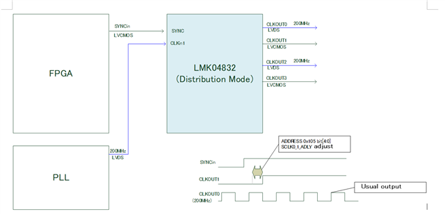
FPGA → connect to LMK04832 SYNC pin
PLL → input 200MHz LVDS to CLKin1

Can I adjust the output delay of the FPGA as above?

Thanks.
Regards,

  • Hello FRANK1,

    To be clear, you are asking:

    • Can the SYNC pin output be buffered through CLKout1 (and other clocks) in distribution mode - Yes, this works
    • Does the SCLKx_y_ADLY adjust the output when buffered like this - This also works, but probably not to the magnitude you want (only ~1ns total ADLY)

    You can also use the SCLKx_y_DDLY and SCLKx_y_HS in distribution mode; the DDLY clock will just be the 200MHz signal. It looks like you are trying to adjust the SYNC signal so that CLKout1 rising edge is isochronous with CLKout0 falling edge. If you are okay with waiting a few 200MHz cycles from SYNC signal to CLKout0 signal (since SCLKx_y_DDLY must be set to a non-bypass value), SCLKx_y_HS will offset the CLKout1 output to exactly the falling edge of CLKout0.

    Regards,

    Derek Payne

  • Hi Derek,

    Thank you for your response.
    I wanna confirm more information.
    -clkout1 output (check agian)
    Input and output to SYNCpin from FPGA,
    It can get output to clklout1 according to my attached diagram, right?

    -SCLKx_y_HS
    Register 0x104 etc in Datasheet Page55 .
    "1: Adjust device SYSREF phase -0.5 clock distribution path cycles."
    means shift 0.5 clocks (2.5ns (200MHz)), right?

    -SCLKx_y_DDLY
    Table3 . DCLK_DIV_ADJUST in Datasheet Page35.
    What do these values mean?

    Thanks.

  • FRANK1,

    -clkout1 output (check agian)
    Input and output to SYNCpin from FPGA,
    It can get output to clklout1 according to my attached diagram, right?

    Correct

    -SCLKx_y_HS
    Register 0x104 etc in Datasheet Page55 .
    "1: Adjust device SYSREF phase -0.5 clock distribution path cycles."
    means shift 0.5 clocks (2.5ns (200MHz)), right?

    Correct

    -SCLKx_y_DDLY
    Table3 . DCLK_DIV_ADJUST in Datasheet Page35.
    What do these values mean?

    There is some amount of time between when the SYNC signal in the LMK04832 is de-asserted (divider reset condition is cleared) and the digital delay counters begin counting. This time is different depending on the divide value used, so DCLK_DIV_ADJUST values are suggested to help simplify aligning edges on clocks with different divide values. For divide-by-1 case, DCLK_DIV_ADJUST is not important since digital delay cannot change the phase of divide-by-1 (except half-step). In divide-by-1 case the DCLK_DIV_ADJUST table can be ignored.

    Regards,

    Derek Payne