This thread has been locked.

If you have a related question, please click the "Ask a related question" button in the top right corner. The newly created question will be automatically linked to this question.

CDCE62002 Basic Questions

Other Parts Discussed in Thread: CDCE62002, SRC4392, PCM1792A

Hi,

I have seen the recent update to the datasheet for the CDCE62002, and i have a few questions.

REF_IN- Connection

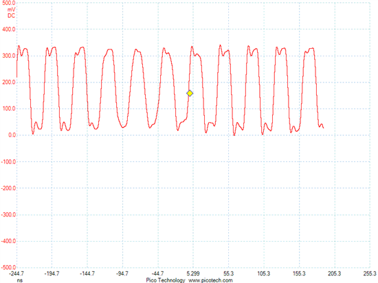
In error i connected the Oscillator to the negative pin of Ref - the REF_IN- which is pin 30, and tied low the Pin 29 - As i have selected CMOS. 

My USB Oscilloscope has a fault on it - so cannot guarantee the outputs - which are set to CMOS.

Is the connection of the REF_IN- pin to the oscillator an issue as the waveform output by the oscillator (24.576MHz) is not looking optimal - positive plateau seems to be ok, but negative is nearly a saw tooth. I have about 3mm of ground plane along one side of the track and obviously tracks either side after this as IC dimensions dictate this for 2mm to 3 mm.


AUX_IN Connection

I have connected a 28.224MHz crystal to the AUX_IN connection. There is a ground plane either side of this track for 7mm before the track is free besides other side tracks to the pin connection. Again, the USB Oscilloscope has a problem, but i do not see any signal on this pin at all - i would have expected there to be some voltage waveform. I believe i had programmed at the time of measurement that the CDCE62002 is to use the AUX_IN pin, so a waveform should be seen ?.


I am not seeing any output on the CDCE62002 and the PLL_LOCK pin seems to indicate a lock issue - hence is the Oscillator waveform too distorted for an adequate reference, and is the track layout for the crystal input outside tolerances for the use of the AUX_IN use - not asking for definitive yes or no, but guidance if this could most probably be the issue. Thanks.

Regards,

Richard

  • Hi,

    As an update - i checked the oscillator output capability - the maximum capacitance that can be seen is 15pF. The x1 probe setting has a capacitance of 46pF + Oscilloscope - hence in excess of the output capability of the oscillator.

    The x10 setting has a capacitance of 11pF and the waveform looks much better - not perfect, but the input capacitance of the CDCE62002 being 3pF means that the load is near a maximum. Hence removing the probe 11pF will resolve the waveform issue.

    The diagram in Figure 23 on page 26 shows that the Positive input pin (29) connects to the Universal Input Controller.

    I have used the Negative Input pin (30).

    Given the connection indicated in Figure 23 shows that the Positive input pin (29) only connects to the Universal Input Controller, and selecting CMOS as the Input Buffer Mode, then any connection to the Negative Input Pin (30) will NOT work at all for a CMOS Input Buffer Mode ?. .

    If anyone can confirm this - i would be most grateful. The PLL_LOCK pin is at 0.9volts hence i assume that this is the reason.

    I have used the following register settings :

    Register 0 : 0E006F75

    Register 1 : 8485D9C1

    I have a 24.576MHz Oscillator, hence with the following settings - can some confirm i have this right - at least ( :O( )

    F=240, I=10, R=1, P=3, Feedback Bypass=1, Output_0=16 (provides 36.864MHz), Output_1=24 (provides 24.576MHz).

    CMOS Output selected, No signals on any output - static 2.1v, 1.7, or 3.3v.

    Hence i believe that i meet the frequency criteria for the PLL etc.

    I did not want to rework the PCB - as it will take quite some time to remove non SMD components to get to the Oscillator area and change the tracks etc. if the above settings are OK and there is another issue with the design or the CDCE62002.

    Thanks and regards,

    Richard.  

  • Hi,

    I noticed the comment on page 34 that VCO Calibration is required after changing the PLL settings etc. Hence as above i set the register values as follows :

    Register 0 : 0E006F75

    Register 1 : 8485D9C1

    Register 2 : 40104080

    Register 2 : 40104080

    Register 2 : 40104010

    Register 2 : 40104080

    Register 2 : 40100080

    To calibrate the VCO.

    Then i completed the following to synchronise the Outputs :

    Register 2 : 40180080

    Register 2 : 40100080

    Register 2 : 40180080

    Before calibration was ever implemented the CDCE62002 was always very hot to the touch - possibly 60deg Centigrade

    After Calibration and Synchronisation the CDCE62002 was ambient temperature.

    1. If the CDCE62002 is NOT calibrated or outputs synchronised - is there a race round condition that consumes excessive current and hence causes the device to warm up ?.

    2. After calibration and sychronisation the MISO output is logic 1 permanently. Is this correct ?. (should be high Z if NOT reading ???, SPI_LE = 1).

    3. Still no output clocks - which i assume may be due to the Oscillator connected to Negative REF_IN Pin ???

    Any guidance, confirmation and explanation on the above gratefully received.

    Thanks and regards,

    Richard.

  • The figures above are read Left to Right - as such the Left Hex character is transmitted first - with the 4 Bit hex character MSB transmitted first.

    I have modified the PCB to meet the latest Datasheet.

    1. The device still gets very warm - even after calibration using the !PD pin.

    2. The Register 2 Calibrate sequence does not work - seems to power down the device.

    3. The REG_CAP3 (as per other post) is reading 2.9volts - which i think is in error - this may be why the IC is getting very warm - there is a fault somewhere.

    4. The Clock Oscillator input is acceptable - the GIF image is for a x10 probe - which causes the load capacitance to be exceeded for the Oscillator output :


    Hence once the probe has been removed the waveform should improve.

    Hence can TI feedback if the 2.9volts on Pin 20 which is REG_CAP3 is an indication of an internal fault or incorrect programming ?.

    Both the default and my own programming result in this lower voltage. All other voltages are as expected.

    I have checked the PCB for any shorts etc., not can be located. So is it possible the IC is not working as it should be ?.

    Thanks and regards,

    Richard.

  • Input is 24.576MHz Oscillator.

    Sequence is sent to CDCE62002 MSB = BIT0, LSB=BIT31 (SPI Bits)

    Revised the sequence to toggle the !PD bit in register 2. Hence write sequence is :

    Register 0 : 0E006F75

    Register 1 : 8485D9C1

    Register 2 : 40180000

    Register 2 : 40080000

    Register 2 : 40180000

    CDCE62002 still does not lock. This combination the VCO = 1769.472MHz

    Used the following to allow for the VCO to use a different frequency which is not near the limits :

    Register 0 : 0EC06F75

    Register 1 : 848399C1

    Register 2 : 40180000

    Register 2 : 40080000

    Register 2 : 40180000

    CDCE62002 still does not lock. This combination the VCO = 1966.08MHz

    With the VCO frequency not near the limits of the range - the REG_CAP3 voltage increases to 3.0volts as opposed to 2.8/2.9volts.

    Hence does REG_CAP3 provide the VCO power internally ?.

    All connections to pins 25 and 26 have been removed - as although using internal PLL feedback, was not sure if internal connections were still being affected.

    PLL_LOCK pin is still 0.9volts.

    Hence, does anyone know what could stop the internal PLL locking ?.

    Thanks and regards,

    Richard.

  • I found this web site where someone else was having problems - they state that they had to write to the device multiple times to get the higher frequency VCO working.

    http://billauer.co.il/blog/2010/10/cdce62002-pll-vco-registers-ram-eeprom/

    Is there an idiosyncrasy with the CDCE62002 causing the PLL not to lock ?.

    I have used many capacitors top side and bottom side as per datasheet to decouple the device, i have 4 separate voltage regulators for the device - 500mA each feed, electrolytic, polyester and ceramic capacitors for each power feed also to ensure a clean power supply for each - yet still no PLL lock.

    Clock signal seems to be ok.

    Is there a thermal dependency on the CDCE62002 for PLL locking ?.

    Thanks and regards,

    Richard.

  • I have been checking the voltages - i think there is an error in the Vbb voltage PIN 3.

    I am reading 3.3volts for this voltage Vbb PIN 3 - and i assume that i have selected the LVCMOS setting on the REF_IN. This PIN 3 should read 1.9volts MAX from the datasheet.

    I am cycling the device to Power Down on PIN 6 every 2 seconds - and the Pin 3 Vbb remains at 3.3volts. The EXT_LFP PIN 25 and EXT_LFN PIN 26 toggle between 0.56 volts and 0.76volts - although i have selected the internal PLL filter.

    Does this mean that the CDCE62002 is malfunctioning ?.

    I assume since i have selected the CMOS input setting for REF_IN PIN 29 used, and Internal PLL Filter that the error voltage of 3.3volts on PIN3 is not an issue, and the voltages appearing from within the CDCE62002 on PIN 25 and 26 have no consequence ?.

    If the above and this post indicate that the CDCE62002 is faulty - please can someone let me know so i can either remove (if possible) or supplant a new circuit to pick up the clocks and SPI control settings leaving the existing IC in place but unpowered.

    Thanks and regards,

    Richard.

  •  

    Hi Richard,

    I read all of your postings and it looks like you are facing PLL lock issue. I think device is o.k. , but programming may not be right.

    Please send my your phone number (f-kabir1@ti.com) and I will call you and discuss the issues.


    REF IN  Connection : For LVCMOS  input pin 29 is right pin for the input buffer

    AUXIN Connection; Programming could be the issue

    Thanks,

    Firoj


  • Hi Richard,


    Please see the attached file. I need to understand your programming bits first. You can try with the seetings (attached).

    Given the connection indicated in Figure 23 shows that the Positive input pin (29) only connects to the Universal Input Controller, and selecting CMOS as the Input Buffer Mode, then any connection to the Negative Input Pin (30) will NOT work at all for a CMOS Input Buffer Mode ?. .

    If anyone can confirm this - i would be most grateful

    Yes, with LVCMOS buffer mode, your connection will not work.


    Thanks,

    Firoj

    CDCE62002_register settings.pdf
  • Hi Firoj,

    Thanks for attaching the document - has helped a lot. As per other post i think there is an error in the datasheet March 2011 - Table 6 bit 5 and Figure 23 table - your results indicate Bit 5 should be a 1 and the data sheet indicates 0 for LVCMOS input.

    I sent a word document last night explaining my code generation - i read Left to Right - so with the Bit sequences reversed in your document - match my bit sequences except for the PLL LOCK bits 13 and 14.,  and Bit 23 for High Performance - my error.

    i believe setting bit 5 to a logic 1 has caused the clocks on the output to be generated - good news.... sort of.

    As per your hex code (registers 0, 1, and 2) i implemented the smallest lock detect window. Results are :

    Output 0 N : 16.9MHz,      Output 0 P : 16.9MHz

    Output 1 N : Logic 1 3.3volts.     Output 1 P : 11.3MHz

    PLL Lock = 0.9volts

    Changed bits 13 and 14 to "1 1" to increase lock window size

    Output 0 N : 12.0MHz,      Output 0 P : 12.0MHz

    Output 1 N : Logic 1 3.3volts.     Output 1 P : 8.0MHz

    PLL Lock = 0.9volts

    Hence, not sure if the wider PLL lock window is allowing the PLL to lock at a lower frequency - as the frequency on the outputs decreases if that window is wider.

    I am also not sure about Register 2 - since this is predominantly marked "TI Test Registers. For TI Use Only" - and you have provided Register 2 Hex code for the example i have provided - does this have an impact on the CECD62002 operation ?.

    Hence do you need to test every frequency combination on the outputs using the EVM module such that register 2 details are provided - and as such you need the EVM module to progress any design ?.

    In the diagram in your attached adobe document - Output 1 has a triangle between the outputs - is this the reason for the permanent logic 1 on the Negative Output pin ?.

    I have a stereo microscope so i can check the soldering - i did so yesterday - seemed ok.

    I have 14 different output clock combination pairs - essentially i am using the SRC4392 and PCM1792A in a design that allows the user to change the up and down sample (if required) rate.

    Thanks and regards,

    Richard.

  • Hi Firoj,

    As extra information - the VCO does seem to be drifting to the lower end of the CDCE62002 capability - 12MHz and 8MHz are being seen by the oscilloscope - i assume my scope is working ok - but the 8MHz frequency is lower than the CDCE62002 capability ?.

    I have removed all components from the external Loop Filter connections - and internal settings have been selected - so not sure what is occurring.

    Thanks and regards,

    Richard.

  • Hi Firoj,

    Thanks for your support on this - the CECD62002 is now providing clock outputs at the frequencies required.

    Thanks and regards,

    Richard.