Hi,
In our application, we are using 1 LMK04832 to synchronize 4 ADCs & 1 FPGA at the same time.To feed every ADC, CLKout0/CLKout8/CLKout10/CLKout12 output 1GHz device clock, CLKout1/CLKout9/CLKout11/CLKout13 output 15.625MHz continuous SYSREF clock.To feed FPGA, CLKout4/CLKout6 output 250MHz device clock(which is connected to FPGA's MGTHREFCLK input), CLKout5/CLKout7 output 15.625MHz continuous SYSREF clock(which is connected to FPGA's SYSREF input), CLKout2/CLKout3 output 250MHz system clock(which is connected to FPGA's logic). For LMK04832, we are using 125MHz clock to feed CLKin2, while it is working at PLL2 Single Loop Mode with running VCO1 at 3GHz. The PDF of PLL2 is configured as 125MHz. And we select the output of N Prescaler to source the N Divider of PLL2(the schematic is attached at last).
For establishing fixed deterministic phase relationship of the phase of the SYSREF output to the phase of device clock output, and also generating all device clock outputs before SYSREF is turning on, we'd like to use SYNC/SYSREF_REQ pin(the rising edge of SYNC/SYSREF_REQ is used as the triger) to turning on continuous SYSREF generation at any time after the device clock generated steadily.
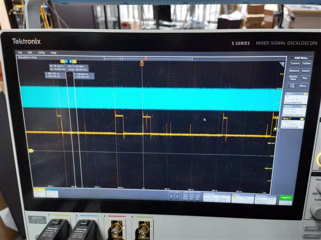
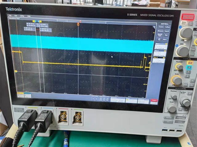
Now we have programed LMK04832 as the following recommanded programming sequence(the configuration file is attached at last). But after the rising edge of SYNC/SYSREF_REQ is asserting, we found that the phase relationship of SYSREF to device clock is changing dynamically(the realtime waveform, which is recorded as mp4 video, is also attached at last). So how can we achieve the fixed deterministic phases? Whether the programming sequence is wrong or the register value is wrong?
Furthermore, when we enable the SYSREF analog delay function, while enabling more than two channels, the frequency of continuous SYSREF clock is changed to low frequency clock unreasonably, which is undesirable and instable. So should LMK04832 be capable of running multiple channels of SYSREF analog delay modules at the same time? If so, how can we implement this function in our design.
; ROM_INIT coe file
; Content :
;

memory_initialization_radix = 16 ;
memory_initialization_vector =

; HIGH = address
; LOW = DATA

; =============================
; 1-a: prepare for manual sync : sync_pol = 0, sync_mode = 1; sysref_mux = 0
; =============================
014301
013900

; =============================
; 1-b: setup output dividers as per example
; =============================
010003
01080C
01100C
01180C
012003
012803
013003
010200
010A00
011200
011A00
012200
012A00
013200

; =============================
; others
; =============================
010744
010F11
011711
011F11
012744
012F44
013500
013744
013824
013F80
014100
014200
014500
014618
01470A
014802
014902
014A00
014B06
014C00
014D00
014EC0
014F7F
015001
015102
015200
015300
015478
015500
015678
015700
015896
015900
015A78
015BD4
015C20
015D00
015E1E
015F0B
016000
016101
01624C
016300
016400
01650C
016958
016A20
016B00
016C00
016D00
016E13
017310
017700
018200
018300
016600
016700
01680C

; =============================
; 1-c: setup output dividers as per example
; =============================
013A00
013BC0

; =============================
; 1-d: setup SYSREF
; =============================
014008
014311
013E01
010420
010C10
011420
011C20
012420
012C20
013420

; =============================
; 1-e: clear local SYSREF DDLY
; =============================
014391

; =============================
; 2-a: set device clock and SYSREF divider digital delays
; =============================
01010A
01090A
01110A
01190A
01210A
01290A
01310A
013C00
013D08

; =============================
; 2-b: set device clock digital delay half steps
; =============================
010340
010B40
011340
011B40
012340
012B40
013340

; =============================
; 2-c: Set SYSREF clock digital delay as required to achieve known phase relationships
; =============================
010602
010E01
011601
011E01
012602
012E02
013602

; =============================
; 2-d: To allow SYNC to affect dividers
; =============================
014400

; =============================
; 2-e: Perform SYNC by toggling SYNC_POL = 1 then SYNC_POL = 0
; =============================
0143B1
014391

; =============================
; 3-a: Prevent SYNC (SYSREF) from affecting dividers
; =============================
0144FF

; =============================
; 4-a: Release reset of local SYSREF digital delay
; =============================
014311

; =============================
; 5-a: Allow pin SYNC event to start
; =============================
014311

; =============================
; 5-b: Select Continuous as SYSREF signal
; =============================
013912