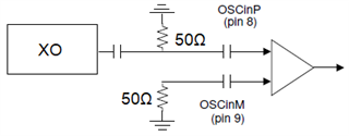
Hi team,
My customer is evaluating our LMX2592 for their design and not sure whether the input waveform as below meets our LMX2592's spec.
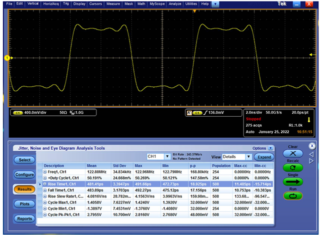
Please refer the input clock as below figure.
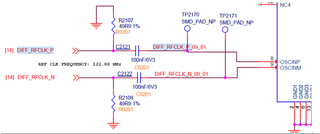
Hi team,
My customer is evaluating our LMX2592 for their design and not sure whether the input waveform as below meets our LMX2592's spec.
Please refer the input clock as below figure.