This thread has been locked.

If you have a related question, please click the "Ask a related question" button in the top right corner. The newly created question will be automatically linked to this question.

LMK04832: LMK04832, LMX2615, DAC5670 & ADC12DJ3200

Part Number: LMK04832
Other Parts Discussed in Thread: LMX2615-SP,

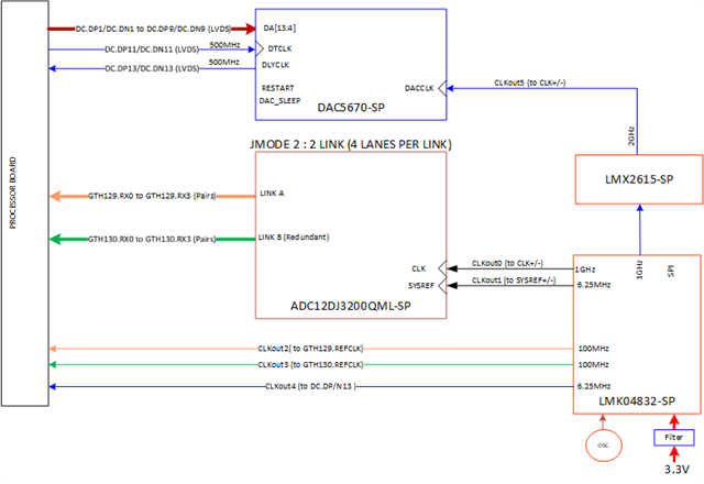
We are designing a Board for Space to be used in a Northrup Grumman space vehicle.    Can you take a look at this and tell me if this will work for the CLK for both the DAC and ADC.    The one thing to note is the DAC uses a 2GHs DACCLK and the data only get clocked into the A port only using the DLYCLK/DTCLK which would mean a 1GHz Data rate.   

  • Hi John,

    From the clocks perspective, the provided configuration looks good, where OSCin frequency to LMK04832-SP need to be selected (say 100MHz) for required output frequencies.

    Also LMX2615-SP can have OSCin input from OSCout (input reference bypassed) or divided DCLKout of LMK04832-SP.

    If there is any critical phase noise/jitter requirement for DAC CLK and/or ADC CLK, I would be suggesting to use PLLatinum SIM tool to simulate phase noise performance for requirement frequencies.

    Regarding the DAC LVDS data rate, I would be suggesting to write to DAC support team. They can help you to provide the answer to your queries.

    Thanks!

    Regards,

    Ajeet Pal  

  • We planned on using 33MHz as the Input Oscillator frequency to the LMK04832.   We have an engineer working with the development boards to get the configuration for these frequencies.  He think that 33MHz will work for all of these frequencies, is he correct?

    Thanks for your response.  

  • Hi John,

    33MHz OSCin frequency doesn't look good for PLL2. LMK04832 has integer PLLs and for 1GHz clock out, VCO frequency should be 3GHz which can be selected for integer division OSCin frequency.

    If possible share the updated configuration file to have a look and will provide my comments.

    Thanks!

    Regards,

    Ajeet Pal

  • The actual frequency is (100/3) = 33.3333... MHz.   So I think we can get all the frequencies using integers.     To get 1G you  Multiply by 30,  to get 500MHz Mult by 15, and to get 6.25MHz  multiply by 3 then divide by 16.      Does this make sense?  

  • Hi John,

    If you have very fine resolution 33.333333333MHz reference frequency, it could make sense and can lock the PLL for 2999.99999MHz VCO frequency. but it may have slightly drift frequency. Otherwise, I would be suggesting to keep the integer reference/OSCin frequency and choose the VCO 3GHz.

    Thanks!

    Regards,

    Ajeet Pal

  • Hi Ajeet,

    As a follow up to the question above:

    The RF output will be from 650-850MHz.

    (DAC clock = 2 GHz and using the A port only)

    Referring to 8.4.1 referenced below, which input mode would you suggest?

    A_ONLY: Input Rate 1 GHz (Signal in the 2nd Nyquist Zone).

    A_ONLY_INV: 2x interpolation, Input Rate 2 GHz. (Signal in the 1st Nyquist Zone).

    A_ONLY_ZS:  2x interpolation, Input Rate 2 GHz. (Signal in the 1st Nyquist Zone)

    What is the difference between  A_ONLY_INV and A_ONLY_ZS and why would we use one over another?

    Would there be an advantage to operate in the 1st or 2nd Nyquist Zones?

    8.4 Device Functional Modes

    8.4.1 Input Format

    The DAC5670 has four input modes selected by the four mutually-exclusive configuration pins: NORMAL, A_ONLY, A_ONLY_INV, and A_ONLY_ZS. Table 1 lists the input modes, input sample rates, maximum DAC sample rate (CLK input), and resulting DAC output sequence for each configuration. For all configurations, the DLYCLK_P/N outputs and DTCLK_P/N inputs are DACCLK_P/N frequency divided by four.

    Thanks.

    Paul

  • Hi Paul,

    Thanks for your query. This query is related to DAC and I would be suggesting to write to DAC support team. They can help you to provide the answer to your queries.

    If you have any question related to clocks, feel free to write here or open a new thread.

    Thanks!

    Regards,

    Ajeet Pal