This thread has been locked.

If you have a related question, please click the "Ask a related question" button in the top right corner. The newly created question will be automatically linked to this question.

CDCI6214: No clock signal on the output

Part Number: CDCI6214


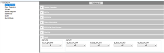
I have a technical support question regarding your CDCI6214 chip. we are using this clock generator to redistribute a single ended 125MHz clock from a phy. We are using the REFP input for the 125MHz signal, as per the datasheet, and have set the registers to get a 125 differential signal on Y1 and Y2 (P and N). The problem is that we aren't getting any clock signal on the outputs. We've used the TICS pro application to make sure that the registers are set so that the signal should be routed correctly. The configuration we use is added below, as I could not find any possibility to add attachments.

  • R70 0x00460000
    R69 0x00450000
    R68 0x00440000
    R67 0x00430020
    R66 0x00420200
    R65 0x00410F34
    R64 0x0040000D
    R63 0x003F4210
    R62 0x003E4218
    R61 0x003D1500
    R60 0x003C0018
    R59 0x003B1061
    R58 0x003A0008
    R57 0x00398851
    R56 0x00380000
    R55 0x0037C001
    R54 0x00360000
    R53 0x00358000
    R52 0x00340008
    R51 0x00338861
    R50 0x00320021
    R49 0x0031C001
    R48 0x00300000
    R47 0x002F8000
    R46 0x002E0008
    R45 0x002D0851
    R44 0x002C0009
    R43 0x002BC001
    R42 0x002A0000
    R41 0x00298000
    R40 0x00280008
    R39 0x00270851
    R38 0x00260009
    R37 0x0025C001
    R36 0x00240000
    R35 0x00238000
    R34 0x00220050
    R33 0x00210007
    R32 0x00200000
    R31 0x001F1E72
    R30 0x001E514A
    R29 0x001D0006
    R28 0x001C0000
    R27 0x001B1801
    R26 0x001A0A1D
    R25 0x00192406
    R24 0x00180000
    R23 0x00170000
    R22 0x00160000
    R21 0x00150000
    R20 0x00140001
    R19 0x00130000
    R18 0x0012FFFF
    R17 0x001126C4
    R16 0x0010921F
    R15 0x000FA137
    R14 0x000E0000
    R13 0x000D0000
    R12 0x000C0000
    R11 0x000B0000
    R10 0x000A0000
    R9 0x00090000
    R8 0x00080001
    R7 0x00070C0D
    R6 0x000619CA
    R5 0x000507FE
    R4 0x00040055
    R3 0x00030801
    R2 0x00020053
    R1 0x00016B88
    R0 0x00000900

  • Hi Peter,

    you have to enable the bits ip_byp_en_ch1 and ip_byp_en_ch2 (or set to 1).

    Field Name: ip_byp_en_ch1

    Register Name: R27
    Start Bit : 11
    Stop Bit : 11
    Length : 1

    Description: Bypass path buffer enable

    Regards,

    Julian

  • Thanks Julian,

    I actually already tried that, by setting 0x1B to 0x1801, but the problem persists.

    Regards,
    Peter

  • Hi Peter,

    please try to set following bits to 0:

    pdn_pll_lockdet

    pdn_pll_vcobuf2

    zdm_mode

    zdm_auto

    regards,

    Julian

  • Thanks,

    I've set 0 to:

    pdn_pll_lockdet & pdn_pll_vcobuf2: 0x020C to reg 0x05

    zdm_mode: 0x0000 to reg 0x00

    zdm_auto: 0xA037 to reg 0x0F

    However, I still get nothing on the outputs.

    I noticed when I follow the guide in the datasheet to write the values to EEPROM, the last step regarding calculating the CRC it is always 0x0000. Also, I see that from the TICS Pro app R3 0x00030801 has the RESERVED 0th bit set to 1, however, the datasheet says 0?

    Do you happen to have any demo apps in C(++) to compile and run on linux to interface the chip over i2c?

  • Hi Peter,

    we don't have a linux app today.

    please try to load this setting (buffer mode with LVDS outputs): 

    R70	0x00460000
    R69	0x00450000
    R68	0x00440000
    R67	0x00430020
    R66	0x00420000
    R65	0x00410F34
    R64	0x0040000D
    R63	0x003F0210
    R62	0x003E4210
    R61	0x003D1000
    R60	0x003C0010
    R59	0x003B0009
    R58	0x003A0008
    R57	0x00390A65
    R56	0x00380005
    R55	0x0037C001
    R54	0x00360000
    R53	0x00358000
    R52	0x00340008
    R51	0x00330A65
    R50	0x00320005
    R49	0x0031C001
    R48	0x00300000
    R47	0x002F8000
    R46	0x002E0008
    R45	0x002D0A65
    R44	0x002C0005
    R43	0x002BC001
    R42	0x002A0000
    R41	0x00298000
    R40	0x00280008
    R39	0x00270A65
    R38	0x00260005
    R37	0x0025C001
    R36	0x00240000
    R35	0x00238000
    R34	0x00220050
    R33	0x00210007
    R32	0x00200000
    R31	0x001F1E72
    R30	0x001E5140
    R29	0x001D000A
    R28	0x001C0000
    R27	0x001B7801
    R26	0x001A8530
    R25	0x00190000
    R24	0x00180000
    R23	0x00170000
    R22	0x00160000
    R21	0x00150000
    R20	0x00140000
    R19	0x00130000
    R18	0x00120000
    R17	0x001126C4
    R16	0x0010921F
    R15	0x000FA0B7
    R14	0x000E0000
    R13	0x000D0000
    R12	0x000C0000
    R11	0x000B0000
    R10	0x000A0000
    R9	0x00090000
    R8	0x00080000
    R7	0x00070000
    R6	0x00060000
    R5	0x000503BE
    R4	0x00040055
    R3	0x00030008
    R2	0x00020053
    R1	0x00016865
    R0	0x00000000
    

    Regards,

    Julian

  • Thanks Julien,

    With those values I do get something on the output! Does this mean that the bypass mode is not functioning?

    I have some questions though, I see that the ref_inbuf_ctrl is set to "AC-Differential", we have a single ended input on REFP, should it instead be set to "LVCMOS"?

  • Hi Peter,

    the setting that I send is in bypass mode. There were likely more bits not set correctly. You should be able to set ref_inbuf_ctrl to "LVCMOS" and chX_outbuf_ctrl to the desired setting.

    regards,

    Julian

  • I tried another device/IC and now I'm able to generate a signal in bypass as well. This leads me to believe that something was set on the other IC to make it malfunction?

    We've compared the default values in the datasheet, and there seems to be discrepancies for the RESERVED fields between the EEPROM1 table and the description in chapter 8. Which one shall we use?

    E.g. POWER1 bit 3 is R/W-0h on p 45, but 1 in the EEPROM1 values.

    Are there any guaranteed working values for the current generation IC and future releases that we can use?

    There are also some other inconsistencies in the datasheet (e.g. I2C-address is stated to be 0x77 with EEPROMSEL high, but is in fact 0x76.)

    The Recommended Programming Procedure description seems also to have a malformed list, where the "Register Commit flow" seems to be misplaced under pt. 7 instead of pt. 1 (page 28.)

    An updated corrected datasheet would be highly appreciated.

  • Hi Peter,

    i will reply shortly.

    regards,

    Julain

  • Hi Peter,

    sorry for the delay.

    All devices that we ship out will have the same EEPROM programming. That is ensured in our final test for each part. If a "fresh" part out of the sample stock works reliable then an undesired EEPROM programming occurred on the other device while testing?

    You already confirmed that the bypass mode works when using the shared register set. That clarifies, that the device itself is not broken. In order to ensure that future devices work correctly as intended for your application, you have to program the EEPROM with the correct values once (if you need to have that functionality at startup. If not, direct register programming every startup is also an option).

    You could for example use the settings that I shared.

    Thanks for pointing out the strange formatting in the 8.5.2 EEPROM Access chapter. I will add that into our datasheet update ticket system.

    Default I2C address: that is known and will be fixed in the next datasheet update to 0x76.

    regards,

    Julian

  • Hi Peter,

    We haven't heard from you long time on this and assumed the issue got resolved. We are closing this thread and you are feel free to reply on this or create new thread for further queries.

    Thanks!

    Regards,

    Ajeet Pal