Because of the holidays, TI E2E™ design support forum responses will be delayed from Dec. 25 through Jan. 2. Thank you for your patience.

This thread has been locked.

If you have a related question, please click the "Ask a related question" button in the top right corner. The newly created question will be automatically linked to this question.

TLC555: 555 Timer as a Switch

Part Number: TLC555

Hi,
I designed a circuit to turn ON and OFF an LED using a vibration switch and a 555 timers. I am facing an issue if someone can help me with it.

I want to turn ON NMOS in normal condition and control LED ON/OFF using a vibration switch which works almost. Now when the gate(Dock Signal port/net) of NMOS is connected with GND then I need to turn OFF the LED until the (Switch port/net) is connected with GND.

The issue is when I connected the gate of NMOS with GND and if LED is glowing then it keeps glowing. Can anyone help me to understand why it is like that? I am using NMOS as a switch.
Thanks


6011.circuit.pdf

  • Hi Ali,

    Can you clarify a few things - your schematic mentions a "SWITCH" node, and also a box that shows a reference designator "SW1".  The "SWITCH" node is the same as the output.  What is the status of "SW1" - are you changing it?  Also, when you mention you pulled the gate of NMOS low, you are referring to the "DOCK SIGNAL" node?

    Also, it doesn't appear that at any point, the value of TRIG/THRESH will go above the THRES comparator voltage (2/3 VCC) because it appears to sit at the middle voltage between two 10kOhm resistors .  I don't understand what the 555 is intended to accomplish here. I suggest building this circuit in TINA SPICE to help understand how the 555 works in this configuration, I think this will help answer the questions here.

    Regards,
    Mike

  • Hi
    Thanks for your reply.

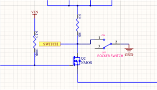
    1. The designator "SW1" is the vibration switch that vibrates to glow LED ON/OFF or make output LOW/HIGH. The "SWITCH" NODE is connected with an external switch one pin whose other pin is directly connected with GND.
    2. YES, when I connect the "DOCK SIGNAL" node with GND then I pulled the gate of NMOS low.
    3. I am trying to use a 555 timer as a push-button circuit. If push button press first time, then glow LED, again press OFF the LED.

    Let me know if you have any further questions.
    NMOS

    SW1

  • I have two goals.

    1. When the DOCK SIGNAL node is logic HIGH then NMOS turns ON and the LED is controlled by a vibration switch.
    2. When the DOCK SIGNAL node is logic LOW then  NMOS turns OFF and the LED is controlled by a SWITCH node using an external switch.
  • Ali,

    Ok, so, the 555 is meant to behave like a latch?  Meaning, when a vibration occurs, the LED is latched "ON", then when another vibration occurs, the LED is latched "OFF"?  

    I see that this basic circuit can be shown in the following link:

    https://circuits-diy.com/simple-latching-circuit-using-555-timer/

    This circuit requires enough of a time period when the switch is open for the capacitor to charge to ground when the output is low, or charge to the supply when the output is high.  Can you measure the VOUT node and the voltage across the capacitor to make sure the capacitor voltage is charging to VOUT? Have you tried the circuit with a push-button switch, similar to the video above, to see if it works with a switch alone?

    What is the equipment that this circuit is being designed for?

    Regards,
    Mike


  • Yes exactly. 
    The latch part is working fine. It works when vibration occurs, the LED ON. Again occur, LED OFF.
    The issue that I am facing is more related to Mosfet maybe. 
    When I connect NMOS gate with GND. It supposes to turn OFF so the latch circuit has no purpose at that stage. In this case, I directly connect the SWITCH node with a GND using an external switch to control the LED.
    Now, the thing which is bothering me is that when I connect the gate to GND then it turns ON the LED(light is not much bright) while it is supposed to disconnect from the OUT terminal of 555 because NMOS is OFF now. Note: The "SWITCH" NODE is OPEN in this case with an external switch(Floating because the external switch is OFF)
    I usually see the NMOS circuit as a switch with gate pull-down while I need the gate to pull up because of the required logic.

    Let me know if you understand the problem I am facing.


  • Hi Ali,

    Ok, I think I understand the problem- when the LED is on, with the NMOS also on, the TLC555 is low.  Then, you shut off the NMOS by pulling the gate to GND, you would expect the LED to turn off since there is now high impedance to GND.  I'm not sure why the LED would not turn off.  Can you verify the voltages on the drain and source of the NMOS in this case?  Are you sure the NMOS is connected correctly?  If the TLC555 timer continues to stay LOW, then I would suspect this has something to do with the NMOS.

    Regards,
    Mike

  • NMOS is connected correctly because it is a SOT-23-3 package and I also checked the pins mapping.
    I noticed the following things.

    1. Never found an NMOS circuit as a switch with gate pull up. Mostly, the gate is pulled down to keep the NMOS OFF while I need opposite to that.
    2. Second, when I connect GATE to GND the LED does not glow at its full brightness but in middle somewhere which indicates that NMOS is not fully turned ON.

    I will send you the voltage details soon.
    Thanks

  • Hi Ali,

    What is the NMOS part number?

    Regards,
    Mike

  • Ali,

    Ok.  Looks like it should be OK depending on what current levels you are expecting through the LED.  The voltages on the FET and across the 10 Ohm resistor will be very useful in debugging.

    Regards,
    Mike

  • Ali,

    The forward voltage of this LED is high.  Do you have 4 of these connected in parallel as shown in the schematic?  The resistor calculator you have above would not apply for that case.   Also, it doesn't account for the drop on the output pin of the TLC555, which may be as high as a volt at 100 mA.  So, a volt on the 10 Ohm resistor, and another on the TLC555, means there is very little conduction through these LEDs.   If there is 4 LEDs, keep in mind the max. current though a TLC555 would be 150 mA absolute maximum; 4*60  = 240 mA would be too high if you were able to increase the headroom.

    Let me know when you've made a measurement on the TLC555, that will be informative.

    Regards,
    Mike

  • Yes, 4 of them are connected in parallel.
    There is one more thing When I turn ON the external switch connected just below the LED resistor the LED glows in full brightness. The problem isn't about brightness for now. The problem is that MOSFET should disconnect the current loop when GND is applied at its gate terminal. When GND is not applied and the gate is connected with a pull-up resistor to a VIN( 3.7 to 5V) which causes the latch circuit to be a part of the current loop then LED brightness and everything works fine with the vibration switch. 

    In short, I need to disconnect the current loop through this MOSFET when GND is applied to its gate. The sole purpose of this MOSFET is to cut down the current path when GND connects with GATE.


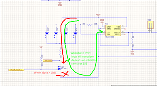
  • I am also sure that When I apply GND at GATE then the above red loop disconnect. The reason is the Vibration switch function does not work. I mean if you vibrate then it does not turn ON/OFF LED instead LED glows continuously with medium brightness. The MOSFET is creating some other path with high impedance for the loop to complete. This is my observation.

    Check this video.
    video.rar

    In video,

    1. Green Wire is Dock Signal NODE in schematic
    2. White wire is SWITCH NODE in the schematic.
    3. The black wire is GND
    4. RED wire is VCC

    When LED glows at battery then their brightness is low which might be due to low battery and we can ignore brightness for now.

    When Green wire connects with GND then I don't need a vibration latch circuit anymore because I will control the LED using white wire by directly connecting them with GND /floating.

  • Hi Ali,

    Unfortunately I'm unable to view the video.  I agree that the NMOS should be OFF, I don't know why it is still conducting.  As I mentioned, voltage measurements will help clarify.

    Note: the abs. max. current on TLV555 is 150 mA sinking, it CANNOT support 240 mA (4 LEDs operating at typical ID).

    Regards,
    Mike