This thread has been locked.

If you have a related question, please click the "Ask a related question" button in the top right corner. The newly created question will be automatically linked to this question.

LMK04616: Generating the register configuration file using TICS Pro

Part Number: LMK04616
Other Parts Discussed in Thread: LMK04610

Hi,

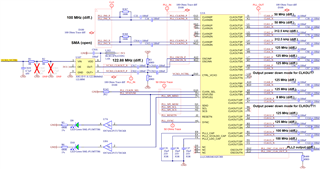
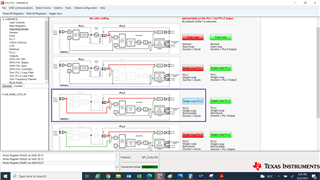
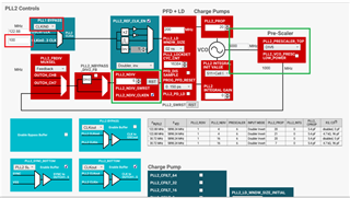
I have a custom board with LMK04616 to generate clocks. It has a 100 MHz TCXO differential clock going as input to the CLKIN0 port, a 122.88 MHz VCXO differential clock input to the OSCIN port, and an optional differential clock input via SMA to CLKIN3 port which is not used at the moment. The configuration and the output clocks desired are indicated in the attached schematic. The registers configurations I tried doesn't seem lock the PLLs for some reason. Please review the schematic for the output clocks to be generated and also for identifying issue, if any. It would be great if I could get the TICS Pro files, .TCS and register values (.TXT) for the output clocks to be generated. Thank you!

  • Hi,

    LMK04616 is an integer dual PLL, which can be operate in dual PLL or single PLL mode. Least common multiple frequency of the required output frequencies would be 500MHz and selected VCO of PLL2 would be multiple of it. Hence, with the 122.88MHz VCXO, required VCO won't be selected. 

    To operate in dual PLL mode, external VCXO frequency should be 100MHz (integer division of 500MHz). With the existing HW, you can operate device in single PLL with CLKin0 100MHz input and can generate required frequencies with 6000MHz VCO frequency.

    Using TICS Pro can select the single PLL mode and modify the PLL2 phase detector frequency, N-divider and output dividers to generate required output frequencies.

    Below is the latest .tcs file for required configuration. Please try with this.

    LMK04616_PLL2only_100MCLKin0.tcs

    Thanks!

    Regards,

    Ajeet Pal

  • Hi Ajeet,

    Thank you for your prompt response. I will try this at our end and let you know the outcome.

  • Hi Ajeet,

    Thank you again for the configuration. I have attached the register .TXT file that I generated used TICS Pro for the desired clock outputs. However, we can only find signal on OSCOut port. Is there a special power-up sequence and also a programming sequence that needs to be followed for properly configuring the device? We have followed the programming sequence mentioned in datasheet chapter 9.5.1. Please note that we have an FPGA that is using the SPI interface to configure the LMK04616 device after boot-up based on the generated .TXT file. Please let us know your thoughts.

    Thank you.

    R0	0x000000
    R1	0x000100
    R2	0x000200
    R3	0x000306
    R4	0x000438
    R5	0x000503
    R6	0x000601
    R8	0x000800
    R9	0x000900
    R10	0x000A00
    R12	0x000C51
    R13	0x000D08
    R16	0x00101E
    R18	0x001204
    R19	0x001310
    R20	0x001400
    R21	0x001508
    R22	0x001648
    R23	0x001711
    R24	0x001802
    R25	0x001903
    R26	0x001A04
    R27	0x001B00
    R28	0x001C64
    R29	0x001D00
    R30	0x001E64
    R31	0x001F00
    R32	0x002064
    R33	0x002100
    R34	0x002264
    R35	0x002314
    R36	0x002480
    R37	0x002514
    R38	0x002680
    R39	0x002714
    R40	0x002880
    R41	0x002914
    R42	0x002A80
    R43	0x002B00
    R44	0x002C10
    R45	0x002D00
    R46	0x002E0C
    R47	0x002F01
    R48	0x003001
    R49	0x00313F
    R50	0x003200
    R51	0x003318
    R52	0x003463
    R53	0x003518
    R54	0x003663
    R55	0x003718
    R56	0x003863
    R57	0x003918
    R58	0x003A03
    R59	0x003B18
    R60	0x003C63
    R61	0x003D18
    R62	0x003E03
    R63	0x003F18
    R64	0x004063
    R65	0x004118
    R66	0x004263
    R67	0x004300
    R68	0x004414
    R69	0x00450C
    R70	0x004680
    R71	0x004700
    R72	0x004808
    R73	0x004900
    R74	0x004A08
    R75	0x004B00
    R76	0x004C08
    R77	0x004D00
    R78	0x004E7D
    R79	0x004F00
    R80	0x005008
    R81	0x005100
    R82	0x00520A
    R83	0x005300
    R84	0x005430
    R85	0x005500
    R86	0x005618
    R87	0x005700
    R88	0x00583F
    R89	0x005930
    R90	0x005A0A
    R91	0x005B32
    R92	0x005C0E
    R93	0x005D00
    R94	0x005E01
    R95	0x005F84
    R96	0x006080
    R97	0x006100
    R98	0x006264
    R99	0x006300
    R100	0x006440
    R101	0x006500
    R102	0x006600
    R103	0x006700
    R104	0x006800
    R105	0x006900
    R106	0x006A0B
    R107	0x006B01
    R108	0x006C01
    R109	0x006D2C
    R110	0x006E1B
    R111	0x006F00
    R112	0x007000
    R113	0x007100
    R114	0x007214
    R115	0x007300
    R116	0x007405
    R117	0x007500
    R118	0x007601
    R119	0x007701
    R120	0x0078FF
    R121	0x007900
    R122	0x007A86
    R123	0x007BA0
    R124	0x007C08
    R125	0x007D00
    R126	0x007E00
    R127	0x007F34
    R128	0x008000
    R129	0x008100
    R130	0x008200
    R131	0x008300
    R132	0x00840F
    R133	0x008501
    R134	0x008601
    R135	0x008700
    R136	0x008840
    R137	0x008900
    R138	0x008A00
    R139	0x008B40
    R140	0x008C00
    R141	0x008D00
    R142	0x008E00
    R143	0x008F40
    R144	0x009000
    R145	0x009100
    R146	0x009280
    R147	0x009380
    R148	0x009402
    R149	0x009501
    R150	0x009610
    R151	0x009720
    R152	0x009820
    R153	0x009980
    R155	0x009B00
    R156	0x009C20
    R157	0x009D00
    R158	0x009E00
    R159	0x009F00
    R160	0x00A000
    R161	0x00A100
    R162	0x00A200
    R163	0x00A300
    R164	0x00A400
    R165	0x00A500
    R166	0x00A600
    R167	0x00A700
    R168	0x00A800
    R169	0x00A900
    R170	0x00AA00
    R171	0x00AB00
    R172	0x00AC00
    R173	0x00AD00
    R174	0x00AE00
    R175	0x00AF00
    R176	0x00B001
    R177	0x00B100
    R178	0x00B200
    R179	0x00B300
    R180	0x00B402
    R181	0x00B500
    R182	0x00B600
    R183	0x00B700
    R184	0x00B800
    R185	0x00B900
    R186	0x00BA3F
    R187	0x00BB0F
    R188	0x00BC50
    R189	0x00BD00
    R190	0x00BE03
    R191	0x00BF00
    R192	0x00C000
    R193	0x00C100
    R194	0x00C200
    R195	0x00C300
    R196	0x00C400
    R197	0x00C500
    R198	0x00C600
    R199	0x00C700
    R200	0x00C800
    R201	0x00C900
    R202	0x00CA00
    R203	0x00CB00
    R204	0x00CC00
    R205	0x00CD00
    R206	0x00CE00
    R207	0x00CF00
    R208	0x00D000
    R209	0x00D100
    R210	0x00D200
    R211	0x00D300
    R212	0x00D400
    R213	0x00D500
    R214	0x00D600
    R215	0x00D700
    R216	0x00D800
    R217	0x00D900
    R218	0x00DA00
    R219	0x00DB00
    R220	0x00DC00
    R221	0x00DD00
    R222	0x00DE00
    R223	0x00DF00
    R224	0x00E000
    R225	0x00E100
    R226	0x00E200
    R227	0x00E300
    R228	0x00E400
    R229	0x00E500
    R230	0x00E600
    R231	0x00E700
    R232	0x00E800
    R233	0x00E900
    R234	0x00EA00
    R235	0x00EB00
    R236	0x00EC00
    R237	0x00ED00
    R238	0x00EE00
    R239	0x00EF00
    R240	0x00F000
    R241	0x00F100
    R242	0x00F200
    R243	0x00F300
    R244	0x00F400
    R245	0x00F500
    R246	0x00F600
    R247	0x00F700
    R248	0x00F800
    R249	0x00F907
    R250	0x00FAD7
    R252	0x00FC00
    R253	0x00FD00
    R254	0x00FE00
    R255	0x00FF00
    R256	0x010000
    R257	0x010100
    R258	0x010200
    R259	0x010300
    R260	0x010400
    R261	0x010500
    R262	0x010600
    R263	0x010700
    R264	0x010800
    R265	0x010900
    R266	0x010A00
    R267	0x010B00
    R268	0x010C00
    R269	0x010D00
    R270	0x010E00
    R271	0x010F00
    R272	0x011000
    R273	0x011100
    R274	0x011200
    R275	0x011300
    R276	0x011400
    R277	0x011500
    R278	0x011600
    R279	0x011700
    R280	0x011800
    R281	0x011900
    R282	0x011A00
    R283	0x011B00
    R284	0x011C00
    R285	0x011D00
    R286	0x011E00
    R287	0x011F00
    R288	0x012000
    R289	0x012100
    R290	0x012200
    R291	0x012300
    R292	0x012408
    R293	0x012500
    R294	0x012600
    R295	0x012705
    R296	0x012805
    R297	0x012905
    R298	0x012A0D
    R299	0x012B05
    R300	0x012C0D
    R301	0x012D05
    R302	0x012E05
    R303	0x012F00
    R304	0x013000
    R305	0x013100
    R306	0x013200
    R307	0x013300
    R308	0x013400
    R309	0x013500
    R310	0x013600
    R311	0x013700
    R312	0x013800
    R313	0x013900
    R314	0x013A00
    R315	0x013B00
    R316	0x013C00
    R317	0x013D00
    R318	0x013E00
    R319	0x013F00
    R320	0x014000
    R321	0x014109
    R322	0x014240
    R323	0x014300
    R324	0x014400
    R325	0x014500
    R326	0x01463C
    R327	0x014700
    R328	0x014800
    R329	0x014900
    R330	0x014A00
    R331	0x014B00
    R332	0x014C00
    R334	0x014E00
    R335	0x014F00
    R336	0x015000
    R337	0x015100
    R338	0x015200
    R339	0x015300
    R17	0x001100
    

  • Hi,

    Registers configuration file looks good. There is an power-up sequence mentioned in datasheet section 9.3.9 and you need to follow the same along with programming sequence.

    Have you observed the current increase of the device once you toggle the DEV_STARTUP bit (0 -->1 -->0) R0x11[0] bit?

    Thanks!

    Regards,

    Ajeet Pal

  • Hi Ajeet,

    Thank you for checking the register configuration for us. Yes, I also caught that information on power-up seuence while going through the datasheet and realized some of the power-up sequencing was not done correctly in our firmware. So, we will soon try to implement the right power-up sequence and update the results here.

  • Hi,

    Thanks for the update.

    Regards,

    Ajeet Pal

  • Hi Ajeet,

    We are following most of the power-up sequencing correctly, except for one step that is regarding the state of RESETn pin at power-up. On our custom board, the state of RESETn is undefined at power-up as there is no pull-down. Therefore, RESETn is NOT set to a LOW at power-up. Our logic is setting it to a LOW after all the devices have been powered up and before programming the device including all the subsequent steps. Can this cause the undefined behavior we're seeing at our end? Please let us know your thoughts.

  • Hi,

    The RESETn must be set to low during powering up the device and toggle to high before SPI write. The schematic shown in above doesn't show any connections to the controller side and not clear.

    If the controller has direct RESETn connection to device and have a separate supply, then can make the RESETn line to Low and later can toggle it to high. Otherwise can keep one pull-down resister at RESETn line and observe the level (should be low) and assumed after power up the device, toggle the RESETn through controller.

    See the below thread, it may help you. (similar part LMK04610)

    LMK04610: Impossible to write registers after RESETN is released - Clock & timing forum - Clock & timing - TI E2E support forums

    Thanks!

    Regards,

    Ajeet Pal   

  • Hi Ajeet,

    Thank you. I am sorry I couldn't get back to you earlier. I did want to confirm that the clock outputs are there on probing the coupling capacitors on our board. We were originally looking only at the OSCout which we had configured to switch to PLL2 output with an OSCout divider set to 10 to produce 100 MHz, but that was not seen. This was the reason why we thought it seemed like the LMK device was not getting programmed. Anytime we tried switching to OSCin as the output for OSCout, we could see it. It would be great if you can send us a .tcs file for the configuration for single loop PLL2 with REF as CLKIn0 and OSCout set to PLL2 output with a divider of 10.

    Our issue didn't seem to be a case of not being about to program via SPI. We are able configure the registers using SPI interface.

    Regards.

  • Hi,

    It's good to know, you identified the issue and resolved it.

    Regarding your required configuration, attached is the updated config file for default 122.88MHz input reference at CLKin0 input with OSCout_div 10.

    1641.LMK04616_CLKin0_REF_PLL2_OSCout.tcs

    Thanks!

    Regards,

    Ajeet Pal