This thread has been locked.

If you have a related question, please click the "Ask a related question" button in the top right corner. The newly created question will be automatically linked to this question.

CDCE6214: Behavior on Fall-back mode.

Part Number: CDCE6214


Hi,

My customer has the following questions.  Could you please support us?
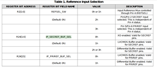
*1.

When my customer wakes up Fall-Back Mode (REFSEL=Open, HW_SW_CTRL=open), which is selected on input clock, PRIREF input or SECREF input?

He plans to connect SECREF pin with 25MHz XO and to connect PRIREF pin with pull-down.  On this case, does "25MHz clock" output from CLKOUT0 pin?

Please advise us.

*2.

Under the above condition, he expects 100MHz diff clock output from OUT2 and OUT3 pins.  Is his understanding correct?

But datasheet said "The PLL would not be auto-calibrated."   What does this mean?  Please advise us.

Thanks and best regards,
M.HATTORI

  • Hello Hattori-san,

    *1.

    When my customer wakes up Fall-Back Mode (REFSEL=Open, HW_SW_CTRL=open), which is selected on input clock, PRIREF input or SECREF input?

    He plans to connect SECREF pin with 25MHz XO and to connect PRIREF pin with pull-down.  On this case, does "25MHz clock" output from CLKOUT0 pin?

    Please advise us.

    Fall-back mode returns to default which shows PIN 4 REFSEL controls reference.  So to select SECREF, please

    Setting REFSEL pin = L selects SECREF input, while setting REFSEL pin = H selects PRIREF Input.  However the IP_SECREF_BUF_SEL default = 0x00, which means XO (should say XTAL mode) is enabled by default.  Should be 0x01 for LVCMOS input or 0x02 or 0x03 as per above for differential buffer.

    Is the 25 MHz XO an LVCMOS output the customer is planning to use?

    *2.

    Under the above condition, he expects 100MHz diff clock output from OUT2 and OUT3 pins.  Is his understanding correct?

    But datasheet said "The PLL would not be auto-calibrated."   What does this mean?  Please advise us.

    We will check this detail and update you.

    73,
    Timothy

  • Hello,

    Regarding PLL calibration, it means that you need to write a "1" to the recal bit to initiate PLL recalibration, after all the other registers are written.

    Regards,
    Hao