This thread has been locked.

If you have a related question, please click the "Ask a related question" button in the top right corner. The newly created question will be automatically linked to this question.

LMK04832: Multi-board Clock synchronization

Part Number: LMK04832


Hi,
 
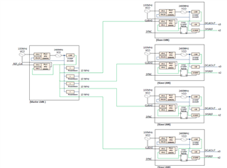
We're using LMK04832 Clock synthesizer for RFSoC FPGA multi-board synchronization.  
  • One Master LMK04832 driving the reference clock (CLKIN0) of 4 slave LMK04832 as attached architecture above.
  • The Master LMK04832 has an input reference clock to CLKIN0 and 100 MHz VCXO input to OSCIN.
  • All slave LMKs will receive CLKIN0 from Master LMK output and have on-board 100 MHz VCXO input to OSCIN. 
  • All 4 slave LMK output clocks need to be synchronized and aligned for Multi-clock synchronization using Zero-Delay Dual-Loop Mode (ZDM), SYNC and continuous SYSREF using SYSREF_MUX mode.

Kindly verify the scheme.

  • Hi,

    The above multi-clock synchronization scheme looks good, where all devices are set for dual loop 0-delay mode and will be synchronizing with input signal and have all slave LMKs outputs are aligned.

    The app note on multi-clock sync may help for further understanding on requirements for 0-delay mode.

    Just an additional comment, if CLKin1 is not utilizing in the system, would be better to keep slave LMKs input at CLKin1 and CLKin0 can be used for SYNC input as it provide very precise sync, if needed in future.

    Thanks!

    Regards,

    Ajeet Pal

  • Hi,

    Thanks for your input.

    Each slave LMK's are on different boards with FPGA.

    • If the slave LMKs are reclocked through the CLKIN0, then all the Slave Outputs will be synchronized?
    • If each slave LMKs sync input from FPGA, i.e Slave1 receives at T1, Slave2 receives ay T2, Slave3 receives at T3, Slave4 receives at T4, after the T5 interval  all slave output (share an edge) will be Synchronous to each other?
    • Should Set and CLR of SYNC_ DISSYSREF and SYNC_ DISX happen synchronously? 

  • Hi,

    If the slave LMKs are reclocked through the CLKIN0, then all the Slave Outputs will be synchronized?

    Do you mean to say by reference input at CLKin0? Yes, to use in dual PLL 0-delay mode, all secondary (slave called secondary) LMKs outputs will be synchronized.

    If each slave LMKs sync input from FPGA, i.e Slave1 receives at T1, Slave2 receives ay T2, Slave3 receives at T3, Slave4 receives at T4, after the T5 interval  all slave output (share an edge) will be Synchronous to each other?

    If the devices are configured for 0-delay mode, it doesn't needed to have sync inputs to synchronize. But for other mode, SYNC inputs to each secondary LMK should be at the same time, otherwise each device may reset the divider at different VCO cycle and can't be synchronize.

    Should Set and CLR of SYNC_ DISSYSREF and SYNC_ DISX happen synchronously? 

    SYNC_DISX and SYNC_DISSESREF should be CLR (0) to receives the SYNC input for resetting the dividers and once reset / SYNC done, set to 1 to avoid any other inputs.

    Thanks!

    Regards,

    Ajeet Pal

  • Hi Ajeet,

    Thanks for the clarification.

    in dual PLL 0-delay mode, all secondary (slave called secondary) LMKs outputs will be synchronized.

    If all the slave LMKs are in Dual PLL 0-delay mode and receive a synchronized reference clock, then all the Slave output will be in sync irrespective of SYNC input. Is my understanding correct?

    While going through " Multi-LMK0482x/LMK04832 SYNC ", It's found that these are the suggested cases for Multi LMK SYNC:  

    of which 4a seems to be the suited design.

    If the devices are configured for 0-delay mode, it doesn't needed to have sync inputs to synchronize

    As seen in the above diagram, it's shown as SYNC should also be driven from Master LMK.  What is your view on this, given that all the Slave LMK receive a synchronized reference clock. 

  • Hi,

    If all the slave LMKs are in Dual PLL 0-delay mode and receive a synchronized reference clock, then all the Slave output will be in sync irrespective of SYNC input. Is my understanding correct?

    That's correct. If the device is operating in nested loop Dual PLL 0-delay mode, it doesn't needed any SYNC input. It should follow the 0-delay rules for deterministic phase relationship.

    As seen in the above diagram, it's shown as SYNC should also be driven from Master LMK.  What is your view on this, given that all the Slave LMK receive a synchronized reference clock. 

    From the table, Case4a is using single PLL, whereas your above configuration shows dual PLL architecture. If single PLL used, case 4a should be good and to have SYNC input from primary LMK is always good so it can be used as case 2b in nested dual PLL 0-delay or case4a also.

    For SYSREF out locally control, I would recommend for case 2b, which is similar to your proposed architecture.

    I think, for option 5a also, SYNC is driving from primary LMK only for re-clocked SYSREF.

    Thanks!

    Regards,

    Ajeet Pal

  • Hi,

    It should follow the 0-delay rules for deterministic phase relationship.

    In our case, we will not be able to follow the 0-delay rule since the Slave output clock is user-configurable 

    i.e GCD(CLKin_FREQ, CLKout_FREQ) ≠ CLKin_FREQ. 

    CLKout_FREQ is user-configurable.

    So 4a seems to be best suited for us and Master will be in Dual PLL architecture and Slave will be in single PLL architecture and SYNC input from Master LMK. 

    Please confirm this.

  • Hi,

    If secondary LMKs operate in single PLL and not meting the 0-delay criteria, my recommendation would be use in case 4b, where CLKout channel divider would be reset by re-clocked SYSREF.

    In single PLL operation, CLKout phase noise / jitter performance depends on the reference input frequency and should be higher input / phase detector frequency used for better performance. Hence, you need to have higher CLKin_FREQ for secondary LMKs.

    It make sure the selection of user-configured CLKout_FREQ should be consider the integer channel dividers with selected VCO frequency.

    Thanks!

    Regards,

    Ajeet Pal