Part Number: CDCI6214
Hello,
I would like you to confirm whether I can use following use.
---
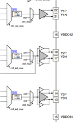
Usecase :
* Input is 25MHz LVDS.
* Output is 2x 125MHz LVDS.
* power supply for all VDDxx is 3.3V.
* use ZDM with internal FB
Q. Is my understanding that we can conpensate between input clock(REFP/N (external reference clock) and both 2 output clock correct ?
(According to datasheet, it seems internal FB mode can be used only for output of ch2. So, in my case when we use ch1 and ch2 as 2 output clock. FB from ch2 output to PLL is available and expect to align input clock phase and 2 output clock phase.(not only ch2 clock but also ch1 clock))
--
BR,