This thread has been locked.

If you have a related question, please click the "Ask a related question" button in the top right corner. The newly created question will be automatically linked to this question.

LMK04821: Clock configuration problem

Part Number: LMK04821

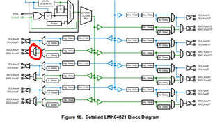
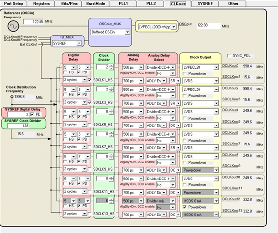
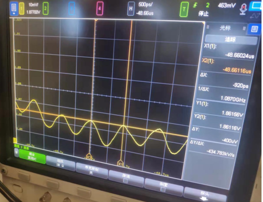
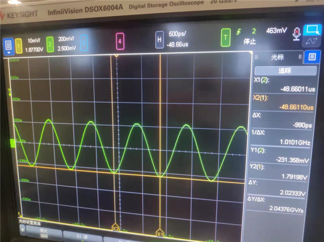
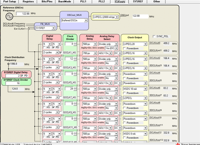
The manual explains that lmk04821 has a total of seven groups of clocks. Each group of clocks includes DCLK and sdclk, of which DCLK is affected by the clock divider parameter and the other sdclk is affected by the sysref clock divider parameter. During debugging, it is found that the output waveform in the same group of clocks is only affected by clock dividers. The configuration is as follows.Coaxial cable connection is dclk0 and sdclk1 respectively.Test with LMK04821EVM.

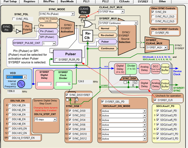
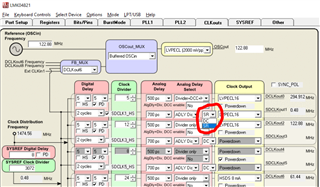
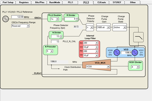
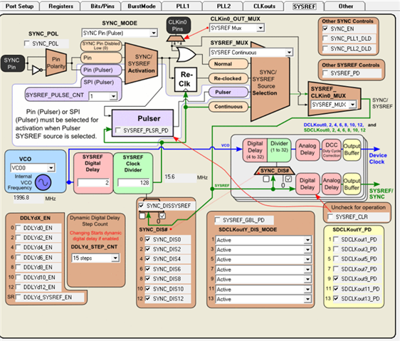
The configuration is shown below.

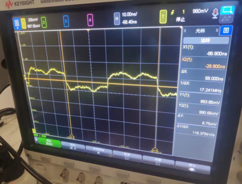
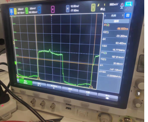
waveform is as follows:

  • Hi,

    SDCLKoutX output frequency depends on the SDCLKoutX _MUX setting, which enables the DCLK output or SYSREF output.

    Ex: For SDCLKout1, 0x104[5] setting should be 1 for SYSREF output enable.

    Thanks!

    Regards,

    Ajeet Pal

  • How to set SDCLKoutX _MUX? I didn't find the specific setting position on the interface

  • Hi,

    If you are using the code loader, you could find the SDCLKout1_MUX field as below.

    I would be preferring to use the TICS Pro tool, which is more advanced and having registers field shown very clear.

    Thanks!

    Regards,
    Ajeet Pal

  • The configuration interface is shown below, and the txt register document is exported in the register export interface, and written into the ROM COE file of FPGA for reading and writing operations.

    Each clock can roughly output, but the frequency changes.

    The first set is 1g and 15.6m respectively,

    The time of EVM evaluation board is 990ps and 63.4ns (green),

    The time of the test board is 920ps and 58ns

    The process, material and temperature of the two boards are different. Do you want to ask the direction of relevant questions.

    It's 1996m now. If adjust to 2G, is there a reference configuration for the whole clock.

  • Hi,

    If I am getting correctly, you wants to have 1GHz output with 2G VCO selection. correct?

    The selection of the VCO frequency based on reference input frequency and PLL2_R and PLL2_N settings. These registers are integer, then to have 2GHz VCO selection, your OSCin input frequency should be integer (say 100MHz), which can lock the VCO at 2GHz.

    I hope, it clarifies your queries.

    Thanks!

    Regards,
    Ajeet Pal