This thread has been locked.

If you have a related question, please click the "Ask a related question" button in the top right corner. The newly created question will be automatically linked to this question.

LMK05028: Outputs do not have fixed phase with REFx

Part Number: LMK05028


Hi, TI team.

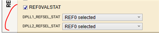
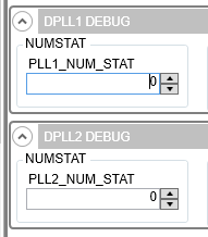
I had a few questions about phase locked. The 4 outputs of DPLL2 have a fixed phase with input clock (REF0) but the other 4 outputs from DPLL1 do not. Until now, we asserted four status (PLL1 Lock Detected, PLL2 Lock Detected, DPLL1 Loss of Lock and DPLL2 Loss of Lock) are all normal. 

I tried to change DPLL phase lock threshold (with register R359 and R360). But it still does not solve the problem.

The questions are:

1.How can I make the phase of DPLL1 locked?

2.Why are the two DPLLs different?

Attached is my configuration file of TICs pro. Thank you and looking forward to your reply.

 8863.lmk05028_config.tcs

  • Hello Maoyuan,

    Until now, we asserted four status (PLL1 Lock Detected, PLL2 Lock Detected, DPLL1 Loss of Lock and DPLL2 Loss of Lock) are all normal.

    My understanding is that 'normal' means that all are locked.

    The 4 outputs of DPLL2 have a fixed phase with input clock (REF0) but the other 4 outputs from DPLL1 do not.

    My understanding is that when you use a scope and probe input and output, the phases are aligned and don't shift.

    1.How can I make the phase of DPLL1 locked?

    2.Why are the two DPLLs different?

    I note you have ZDM enabled for DPLL1 and DPLL2.

    I want to be sure I understand, the DPLL1 output clocks (120 MHz) have a constantly shifting phase with respect to the input 10 MHz clock?  Or do they simply not align (ZDM) as DPLL2 do?

    Is ZDM required?  I suggest disabling ZDM for DPLL1 and re-calculate

    --

    I did just load your .tcs file and recalculate the frequency plan.  I noted that the some of the PLL1 PLL R/N was changed.  Perhaps there is some simple mis-configuration?  I've attached the files I created, please see if these solve our issue.  I've not been able to test them in lab.


    recalc with ZDM on for DPLL1 and DPLL2.tcsrecalc with ZDM off for DPLL1 and on for DPLL2.tcs

    73,
    Timothy

  • Hello, Timothy!

    Thanks for your reply!

    I tried the .tcs file you created, but the issue has not been solved yet. The DPLL1 output clocks (120 MHz) still have a shifting phase with respect to the input 10 MHz clock.

    I tried to read R14 register (Address = Eh) , which shows several flags about DPLL1. The following is the value of R14:

    bit7:LOPL_DPLL1 = 1 <==== indicates loss of phase lock DPLL1

    bit6:LOFL_DPLL1 = 0 <==== indicates frequency of DPLL1 is locked

    The result above shows that the frequency of DPLL1 is locked but the phase of DPLL1 is not locked. 

    The  LOPL_DPLL1 is always 1 even though I set the maximum value (3Fh) of lock threshold (R359 and R360) of DPLL1 Phase Lock Detectors.

    And I also to read R15 register (Address = Fh) , which shows several flags about DPLL2. The following is the value of R15:

    bit7:LOPL_DPLL1 = 0 <==== indicates phase lock DPLL2 is locked

    bit6:LOFL_DPLL1 = 0 <==== indicates frequency of DPLL2 is locked

    The result above shows that the frequency and the phase of DPLL2 are both locked.

    So how can I make DPLL1 phase locked?


    I have another question: 

    There are two status signals called:

    DPLL1 PathA R Divider, div-by-2 (R46 register, address = 2Eh, value = 40h)

    DPLL1 REF N Divider, div-by-2 (value = 41h) 

    Now the frequency of the two signals are both 500kHz and DPLL1 PathA R Divider has a shifting phase with respect to DPLL1 REF N Divider when I use your .tcs file. 

    What do the two signals mean?

    Thank you and looking forward to your reply.

    Yours,

    Maoyuan


  • Hi Maoyuan,

    I'll review your response more closely later, but I did confirm that DPLL1 from your config was unable to lock in my lab.  I was able to get the configs I shared to lock in the lab.  I did have a trouble with my reference input such that I had to disable the reference validation to get the DPLLs to lock, I may have needed to use a differential input... I'll check more on that.

    Can you confirm in all cases your REF0 is validated?

    73,
    Timothy

  • Hi, Timothy!

    I have confirmed that my REF0 is validated when I disabled the frequency detect. If I enable the frequency detect, REF0 is invalid and two DPLLs are both unlocked.  If I disable the frequency detect, DPLL1 is unlocked but DPLL2 is locked.

    I tried to config the .tcs files you sent to me yesterday. I noted that you set the DPLL1 R divider to 26 and set the DPLL2 R divider to 2. After I config, I read the R306 and R307 register to check the DPLL1 R divider. But it is still 10 (the value in .tcs file before), not 26. I checked other registers and found the values of the four registers about DPLL1 (as figure shows) are not changed.

    Here the values in the figure are from your .tcs file. But the values I read from register thru SPI are not changed after I config.

    I tried to soft-reset chip and soft-reset PLLs. But it is still not changed. Please tell me how to change the registers above? I might use a wrong sequence.

    Thank you and looking forward to your reply.

    Regards,

    Maoyuan


  • Hi Maoyuan,

    I apologize for the extreme delay.  I hope you've managed to resolve this issue.

    I have confirmed that my REF0 is validated when I disabled the frequency detect. If I enable the frequency detect, REF0 is invalid and two DPLLs are both unlocked.  If I disable the frequency detect, DPLL1 is unlocked but DPLL2 is locked.

    If disabling the frequency detect, REFx becomes valid because there is nothing to prevent it from validating.  If there is an issue with ref validation setting but the input is otherwise good.  Then this could allow the DPLL to lock.  In your case it appears DPLL2 is able to lock but DPLL1 is not.

    See the info on debugging using PLLx_NUM_STAT below, this would be interesting to see how DPLL1 vs. DPLL2 is behaving.

    Here the values in the figure are from your .tcs file. But the values I read from register thru SPI are not changed after I config.

    So you are advising that after TCS load, you see the updates, but then after programming.  When you do a readback they revert to previous values?  This is unusual.

    After loading the .TCS, you may try pressing "Ctrl+L" to load all registers.  This should force the values to take effect.  You could then do a soft-chip reset to re-start the PLLs with those new values.

    Here the values in the figure are from your .tcs file. But the values I read from register thru SPI are not changed after I config.

    Can you use test with I2C interface?

    --

    Debug using PLLx_NUM_STAT

    I wanted to mention one other debug method... when the DPLL is not in holdover, the DPLL should be updating the APLLx numerator to keep locked to the input reference.  The actual momentary value is able to be read back from PLLx_NUM_STAT.  These are located on the User Controls page at the bottom in the DPLL1 DEBUG and DPLL2 DEBUG shade:

    To perform the readback, click the control to give focus (PLL1_NUM_STAT has focus above), then press Ctrl+R.  This will perform readback.  Repeated press this to see the value change.  Note the nominal frequency that the DPLL as tuned to can be calculated by using this PLLx_NUM_STAT value as the APLLx numerator and calculating XO ref / APLL R * APLL XO doubler * APLL Total N.
      > APLL R is = 1.  APLL XO doubler is 1 if doubler not enabled or 2 if enabled.

    73,
    Timothy