This thread has been locked.

If you have a related question, please click the "Ask a related question" button in the top right corner. The newly created question will be automatically linked to this question.

LMK04828: Custom Board LMK04828 Phase noise level

Part Number: LMK04828

Hi 

We have a custom board with LMK04828 and RFSoC.

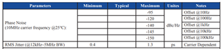
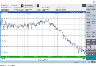
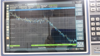
We are observing Phase noise of LMK output to be very less around -95 to 100 dBc/Hz at 1K to 100KHz offset

Due to this, RF DAC Outputs also have same Phase noise.

Below attached schematic of LMK Section:

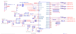
We have tried changing Loop filter CP1 values of C622 to680nF, C623 to100nF and R402 to 39K. Still the same result of phase noise.

Please suggest us how we can improve the phase noise.

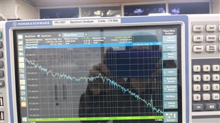
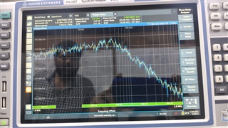
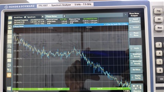
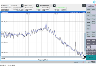
Below attached Phase noise for reference.

Phase noise of VCXO 100MHz (Y10)

Phase noise of LMK Output (DCLKOUT6)- 256MHz

Phase noise of DAC Output (440MHz)

  • Hello Lakshminarayana,

    Can you provide the register programming? Your loop bandwidth looks very low on PLL2, and I'm not sure how PLL1 is configured. With the register programming, I should be able to check the loop filter behavior.

    Regards,

    Derek Payne

  • Hi Derek,

    Thanks for your immediate response,

    please find the attachment of configuration file.

    clkin0 =10MHz, external VCXO = 100MHz  

    R0 (INIT)	0x000090
    R0	0x000004
    R2	0x000200
    R3	0x000306
    R4	0x0004D0
    R5	0x00055B
    R6	0x000600
    R12	0x000C51
    R13	0x000D04
    R256	0x01000A
    R257	0x010155
    R258	0x010255
    R259	0x010301
    R260	0x010422
    R261	0x010500
    R262	0x010670
    R263	0x010755
    R264	0x01086A
    R265	0x010955
    R266	0x010A55
    R267	0x010BB1
    R268	0x010C22
    R269	0x010D00
    R270	0x010E70
    R271	0x010F11
    R272	0x01106A
    R273	0x011155
    R274	0x011255
    R275	0x0113B1
    R276	0x011422
    R277	0x011500
    R278	0x011670
    R279	0x011733
    R280	0x01186A
    R281	0x011955
    R282	0x011A55
    R283	0x011BB1
    R284	0x011C22
    R285	0x011D00
    R286	0x011E71
    R287	0x011F03
    R288	0x012072
    R289	0x012155
    R290	0x012255
    R291	0x0123B1
    R292	0x012422
    R293	0x012500
    R294	0x012678
    R295	0x012755
    R296	0x012808
    R297	0x012955
    R298	0x012A55
    R299	0x012B00
    R300	0x012C02
    R301	0x012D00
    R302	0x012EF9
    R303	0x012F00
    R304	0x013016
    R305	0x013155
    R306	0x013255
    R307	0x013300
    R308	0x013402
    R309	0x013500
    R310	0x0136F1
    R311	0x013700
    R312	0x013805
    R313	0x013903
    R314	0x013A02
    R315	0x013B80
    R316	0x013C00
    R317	0x013D0E
    R318	0x013E03
    R319	0x013F05
    R320	0x014009
    R321	0x014100
    R322	0x014200
    R323	0x014321
    R324	0x0144FF
    R325	0x01457F
    R326	0x014618
    R327	0x01470A
    R328	0x014802
    R329	0x014942
    R330	0x014A02
    R331	0x014B16
    R332	0x014C00
    R333	0x014D00
    R334	0x014EC0
    R335	0x014F7F
    R336	0x015003
    R337	0x015102
    R338	0x015200
    R339	0x015300
    R340	0x01540A
    R341	0x015500
    R342	0x0156C5
    R343	0x015700
    R344	0x015896
    R345	0x015900
    R346	0x015A64
    R347	0x015BD4
    R348	0x015C20
    R349	0x015D00
    R350	0x015E00
    R351	0x015F0B
    R352	0x016000
    R353	0x016105
    R354	0x016245
    R355	0x016300
    R356	0x016400
    R357	0x01650C
    R369	0x0171AA
    R370	0x017202
    R380	0x017C15
    R381	0x017D33
    R358	0x016600
    R359	0x016700
    R360	0x016820
    R361	0x016959
    R362	0x016A20
    R363	0x016B00
    R364	0x016C00
    R365	0x016D00
    R366	0x016E13
    R371	0x017300
    R386	0x018200
    R387	0x018300
    R388	0x018400
    R389	0x018500
    R392	0x018800
    R393	0x018900
    R394	0x018A00
    R395	0x018B00
    R8189	0x1FFD00
    R8190	0x1FFE00
    R8191	0x1FFF53

  • Hi @

    Attaching below TCXO 10MHz (Y9) Phase noise.

    Few experiment carried out:

    1. Made PLL1 PD1 at 0.1MHz and observed VCXO,LMK Output clock with charge pump gain set to 150uA and 450uA.
    2. As previously mentioned, the values for the CP1 filter were changed from C622 to 680nF, C623 to 100nF, and R402 to 39K. The phase noise result is still the same.
    3. Made PD2 as 100MHz for VCO0 of 2500MHz, LMK Output was 250MHz

    All of this resulted in similar phase noise at LMK output.

    Please advise on how we can reduce phase noise.

  • Lakshminarayana,

    I do see that the register programming has FB_MUX_EN=1, which is driving the 4 MHz continuous SYSREF to the NCLK muxes - this may be introducing some noise in the feedback path, but I'd be surprised if this was the primary source of the noise.

    It's notable that the shape of the phase noise on the TCXO and the shape of the phase noise on the LMK are so similar. The 10 MHz TCXO phase noise looks astonishingly high, around 30 dB higher than what I would expect based on the part number in the schematic. The phase noise performance from the TCXO datasheet suggests you should be seeing -140 dBc/Hz at 1kHz offset; clearly your plot is well above this.

    I can think of a few possibilities:

    • TCXO is malfunctioning, and not performing to spec. The TCXO noise is so high that even the PLL1 loop filter is unable to completely suppress it, and reference noise is scaling through your whole system. This could be tested by validating a TCXO that performs according to your specs, and providing it from off-board to the other clock input.
    • You may have a switching supply or something similarly disruptive on the power supply and grounding for the TCXO or VCXO that is injecting broadband noise. This could be validated with a clean 3.3V supply if you suspect something like this is happening, but if you don't have switching noise, CMOS circuits switching in-band, or other sources that might be coupling broadband noise into your board, this might not be a likely problem.
    • The spectrum analyzer you are using may have a fundamental measurement limitation - check the datasheet for the analyzer and confirm that it can actually measure the phase noise you need to see at the frequencies you are measuring.

    Regards,

    Derek Payne

  • Hi 

    Thanks for your inputs.


    1. Made PD2 as 100MHz for VCO0 of 2500MHz, LMK Output was 250MHz

    This was done using the on-board VCXO in PLL2 mode, and the phase noise was similar.

    We have tried with PLL2 mode and disabled PLL1, as well as an external VCXO of 100MHz (Part: CVSS-945-100.000).

    The phase noise are shown below, and  is still not good.

    VCXO Phase noise (CVSS-945-100.000)

    LMK Out Phase noise

    You may have a switching supply or something similarly disruptive on the power supply

    How do we remove the low frequency noise(~48KHz) on the supply?

  • Hi 

    Awaiting for your feedback..

    Thanks.