This thread has been locked.

If you have a related question, please click the "Ask a related question" button in the top right corner. The newly created question will be automatically linked to this question.

LMK04803BEVAL: Request for LMK04803 evaluation board schematic and design files

Part Number: LMK04803BEVAL
Other Parts Discussed in Thread: LMK04803, LMK04832

Hello support team,

We are planning to use LMK04803 clock synthesizer IC to provide reference clock to TLK2711 SERDES transceiver. I am looking for the schematic of the LMK04803 evaluation board that I can taken as a reference. I do not find it in the website, Can you please provide the same. Also, when using this LMK04803 for TLK2711 SERDES clock , is there any suggestions that you could provide which needs to keep in mind , then it would be very helpful for us.

We are considering this LMK04803 as it has very low RMS jitter up to 111 femto sec. 

  • Hello,

    I have found the schematic , which is inside the eval board instructions. I have some queries regarding the use of LMK04803 Clock synthesizer as below.

    1. My output frequency requirement from LMK04803B is 110 MHz. For which I have tried different combinations using clock design tool for the generation of 110 MHz LVCMOS output. 

    I am planning to use same frequency VCXO for PLL1 input as well PLL2 input as taken reference from the standard 122.88 MHz crystek(commercial VCXO use) in the datasheet. 

    For the generation of 110 MHz LVCMOS, In lower standard frequency : 20,10 , 19.8 MHz are possible, while for higher standard frequency : 60 MHz, 220 MHz are possible. 

    My main aim is to select the reference input source , which in turn can have lowest possible jitter for 110 MHz LVCMOS output.( as given in the datasheet for the crystek 122.88 MHz oscillator) .

    What I found in the commercial available VCXO is that for lower frequency(like 20 MHz) , jitter performance is not good. with high frequency, it is possible to have good rms jitter performance . 

    So, In order to have final RMS jitter for the 110 MHz LVCMOS output in the range of 111 femto second, the recommended reference clock should be high only, like 220 MHz or is it possible to have low rms jitter of 111 femto sec with the lower frequency clock source like 20 MHz ?

    Request you to kindly share your guidance and support on the selection of Clock source (in terms of frequency) , so that we can achieve ultra low rms jitter performance for final clock out from LMK04803.

  • Hello support Team,

    Awaited your feedback and guidance on the above. 

  • Hi Maitry,

    sorry for the delay here.

    What is the input frequency that you will provide to PLL1.

    Using 122.88MHz VCXO for PLL1 and as input to PLL2 is not recommended, if you need 110MHz output. For 110 MHz output you need to use 1980MHz VCO frequency on PLL2. With that the you can use a 110 or 99MHz VCXO.

    Note, both PLLs in LMK0480x family are integer-N PLLs.

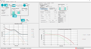
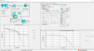
    With LMK04803 you will achieve around 140fs rms output jitter for a 110MHz clock:

    LMK04832 brings you below 100fs rms (10kHz to 20MHz):

    regards,

    Julian

  • Hello, 

    With LMK04803 , What I understand from your response is that , We need to use 110 MHz commercial available VCXO at the input of PLL2 as well at the input of PLL1 (reference clock) , which we can use from crystek,

    By using LMK04803 in dual PLL mode, it will be possible to get 140 fsec jitter. 

    Or can we use only PLL2 by power down PLL1 to use LMK04803 in single PLL mode?

    Please share your views.

  • Hello,

    If you have a clean reference, then you don't need the VCXO based PLL loop (PLL1).

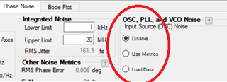
    You can model the phase noise in PLLatinum Sim. Enter you reference Phase noise when modeling PLL2 here (intermediate or advanced mode):

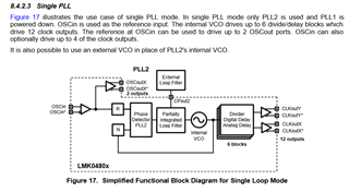
    Yes PLL2 can be used alone:

    Regards,

    Julian

  • Hello Julian,

    Thank you for your accurate response. 

    Yes, got it, In dual PLL Mode, PLL1 is used to clean the input reference clock. 

    So, as I do not have the clean source and I have lower frequency VCXO like 20 MHz and 60 MHz only. So, I am planning to use same 60 MHz vcxo at the input of PLL1 and PLL2 to generate 110 MHz. As it is possible to set 1980 MHz VCO using 60 MHz input reference. 

  • Hi,

    higher VCXO frequencies lead to better output jitter. Please check with PLLatinum Sim if the 60MHz VCXO is good enough for your system.

    Otherwise, yes, you can use the 60MHz VCXO as input to PLL2 to have the VCO at 1980MHz.

    regards,

    Julian