Other Parts Discussed in Thread: LMK04828, ADC12DJ5200RF, LMK04821
Hi Team,
My customer is using LMK04826 provide JESD204C REFCLK for FPGA , but got some problem with JESD204B link,
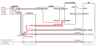
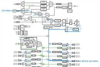
1. The original design(ref. to picture):
FPGA:ZCU106
Clock generator:LMK04826
Source:TCVCXO 125MHz
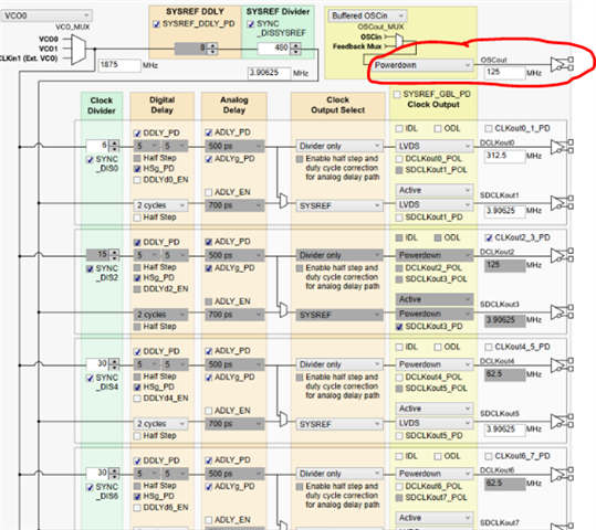
VCO0:1875MHz
REFCLK:VCO0/6=312.5MHz
Sync problem(ref. to picture):use above setting provide REFCLK to FPGA, but Sync waveform is toggle , cannot get JESD204C link
2. customer modify LMK04826 setting below
FPGA:ZCU106
Clock generator:LMK04826
Source:Signal generator 312.5MHz
VCO0:No used
REFCLK:Signal generator Bypass=312.5MHz
Conclusion:provide REFCLKt o FPGA and Sync is always high & JESD204C become link
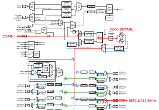
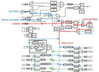
3. modify our to another design as setting below (ref. to picture):
FPGA:ZCU106
Clock generator:LMK04826
Source:TCVCXO 125MHz & Signal generator 312.5MHz
VCO0:1875MHz
REFCLK:Signal generator Bypass=312.5MHz
Conclusion:provide REFCLK to FPGA and Sync is always high & JESD204C become link

below are questions from customer,
1. why 312.5MHz REFCLK divide from VCO0 will cause JESD204C sync. toggle and link can't establish?
2. base on #3 modification, does 125MHz & 312.5MHz need synchronization?
3. customer check our ADC12DJ5200RF EVM+ TSW14J57 reference design, REFCLK is also not divide from LMK04828 VCO, is it correct?
Thanks & Regards
Eddie