This thread has been locked.

If you have a related question, please click the "Ask a related question" button in the top right corner. The newly created question will be automatically linked to this question.

CDCE913 Vctr characteristics

Other Parts Discussed in Thread: CDCE913, CDCE949

Hi,

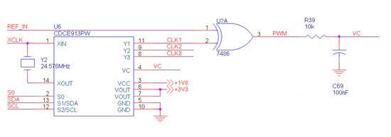
I use a CDCE913 with a simple EXOR PLL and meassure the Vctr voltage with an ADC to calculate phase shift between clock and reference clock. Unfortunately the internal pullup distorts my calculation.

Can someone tell the resistance of the pullup resistor or the current, if a current source is build in, of the Vctr pin? Can I solve this with a smaller resistor (actually 10k) or is it better to build a redundant low pass filter for the ADC.


Thanks in advance

Thomas

  • Hi Thomas,

    the Vctrl pin which is available on the CDCE913, is just an input pin. In case the device is programmed to receive an input from a VCXO, the Vctrl is used to fine tune the oscillation frequency of the VCXO.  For normal operation it should be kept open or pulled-up, like specified in datasheet at page 2.

    Vctrl does not contain any information about phase shift between clock and reference clock and it is not the control voltage for the interval VCO.

    If you need some other info, feel free to contact us.

    Best Regards

    Leandro


  • Hi Leandro

    Thanks for your reply. It looks I was not quite clear again. I know the data sheet. I have a reference clock fed into an exor gate and a VCXO output fed to the same exor gate. At centre this PLL locks with 90Degree phase angle. At the upper limit there is a 180Degree phase angle while at lower limit the phase angle is 0Degree. The low pass filter is a 10k resistor and a 100nF capacitor. Now the phase angle is directly proportional to the control voltage unless nothing pulls the integrator. But this seems to happen and must be taken into account. So I just need to know what the input impedance and current of the vctr pin ist.

    There are several ways to overcome the problem: Buffering the VC so it cannot be pulled by the input, building a second low pass filter that won't be pulled for the ADC or  simply make the circuit lower impedance and accept a small amount of error. Before I start headless soldering on my prototypes I would rather prefer to get the information on the input.

    Do you have an IBIS model of the part? Maybe I can extract this out of the model.

    Thanks

    Thomas

  • Hi Thomas,

    Sorry for late reply. I am checking with the designer about the input impedance of Vctrl pin. We have an IBIS model for the CDCE949, which is the Quad version of the CDCE913. I guess there should not be any problem using that model. But I will check it as well.

    Regards,

    Leandro


  • Hi Leandro,

    Thanks for your reply. I checked the IBIS file but unfortunately the VCTRL pin is not propper defined:

    4         VCTRL          POWER          0.08703   1.05334e-09   0.08277e-12

    It is in the Power class.

    Meanwhile I changed the resistor from 10k to 1k but did not have much difference. It looks like a PCB problem. Maybe I have a ground shift. Anyway, if a designer could give a hint in which region the pullup can be found I could take this into account. I know that those on-die pullups have large tollerances.

    Thanks

    Thomas

  • Thomas,

    yes, the Vctrl pin is defined as power pin in IBIS model. I got the answer from designer. Generally Vctrl pin is very high impedance (> 100k).

    I have one question from my side: did you program the device in VCXO input mode? In that case there is no internal pull-up resistor at all.

    Regards,

    Leandro