This thread has been locked.

If you have a related question, please click the "Ask a related question" button in the top right corner. The newly created question will be automatically linked to this question.

LMK05318BEVM: TICSPRO-SW

Part Number: LMK05318BEVM
Other Parts Discussed in Thread: LMK05318B,

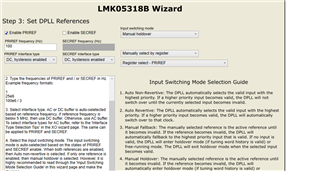
We want to generate some frequencies -- 30.72MHz and 6.912MHz from 100Hz. This 100Hz clock will be generated and given as input to LMK05318B       EVM.
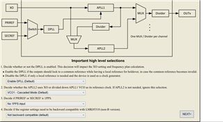
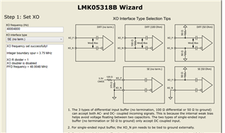
But we are not able to generate the required frequencies.

  • Hi Gurunath, 

    This should meet your requirements.

    LMK05318B_100Hz in.tcs

    Regards, 

    Vicente

  • Hi Vincent,

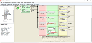
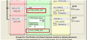
    Our requirement also needs a clock synchronisation with the PRI_REF. On selecting CHx_SYNC_EN in the Advanced -> Outputs section, the outputs is resulting to be disabled. The clock output is as per expected frequency when this selection is unchecked, but the locking of the phase of the input and output is not seen. 

  • Thanks, we will use this configuration file and check

  • Hi Vicente,

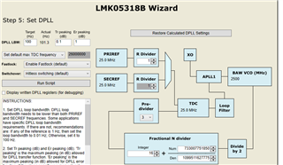
    I checked the .tcs file shared by you, the issue encountered here was during Run DPLL script, LBW of DPW is set to be 100 Hz. Could you suggest an appropriate value for LBW. The output frequency value obtained is as expected, but the phase aligning of these two clock loops is still not possible.

  • Hi Akanksh, 

    Just to confirm, you say when you enable the output channel synchronization, you don't see the output signals on your Oscilloscope? 

    Regards, 

    Vicente 

  • Hi Vicente,

    Yes when I enable the Output channel synchronisation, the don't see the output signals on the oscilloscope.

    I would also like to highlight some more points here:

    1. For the "LMK05318B_100Hz in.tcs" configuration file I get the following error "DPLL loop bandwidth must be less than PRIREF/SECREF frequency". What value of LBW should I configure?

    2. I am checking the clock outputs with the default jumper configurations as mentioned in the LMK05318B EVM user guide. Should I change any of the jumper configuration for the output synchronisation and phase alignment of the two output frequencies.
    3. The output synchronization is only observed with a different configutaion of 5 MHz as PRI_REF and output configured as 10 MHz. The output frequency remains out of phase for any other frequency configuration.

    Regards,

    Akanksh 

  • Hi Akanksh,

    I can take a look at this and provide a configuration tested in lab by the end of the week.

    Regards,

    Jennifer

  • Hi Jennifer,

    Could I get it by tomorrow?

  • Yes, I will share a tcs config by tomorrow.

    Regards,

    Jennifer

  • Hi Jennifer

    The output required for 6.912 MHz and 30.72 MHz is LVCMOS Output.

    Regards 

    Akanksh S

  • Hi Akanksh,

    Please try this configuration: e2e LMK05318B_XO=12.8 MHz_PRIREF=100Hz_OUT=30.72 and 6.912 MHz_Oct 21 2022.tcs.

    • I have confirmed the outputs lock to a 100 Hz DPLL input.
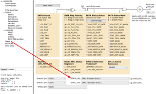
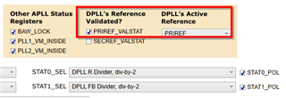
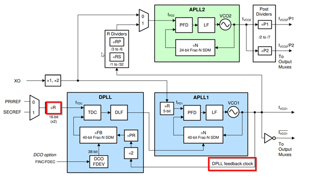
      • This can be also tested by probing the DPLL R and DPLL FB dividers on the STAT0 and STAT1 pins.
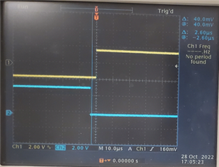
      • See confirmation picture of such STATx signals below:
    • Note that this configuration uses a 12.8 MHz XO input which is recommendable for 100 Hz DPLL reference. Using a lower XO frequency increases the XO ppm accuracy requirement. A 12.8 MHz XO has a +/- 4.92 ppm requirement. 
      • For the LMK05318BEVM, the XO should be powered down by setting J9 to GND. 12.8 MHz frequency can then be connect to J33.
    • It will also take a long time (20+ minutes) for DPLL_LOPL to go LOW due to the narrow (0.1 Hz) LBW.
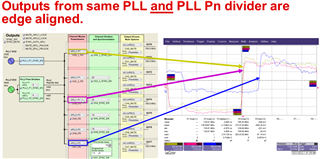
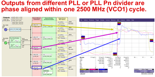
    • Phase alignment is possible across outputs from the same PLL and PLL post dividers after asserting a SYNC. For outputs from different PLLs or PLL Pn dividers, synchronization is possible within 1 VCO (2500 MHz) cycle. Refer to the examples below:

    Regards,

    Jennifer

  • Hi Jennifer,

    I tried the configuration file with 48.0048 MHz and couldn't obtain the output synchronisation. Since the 12.8 MHz output is not readily available currently. Can I use a 12 MHz crystal input for the clock(any hardware changes required on the EVM)? The 10 MHz SE input is available, but not able to configure it to that XO Frequency on the wizard.  

    On reading the status registers, the HLDOVR_INTR is showing as high. what could be the possible reason. The R divider and FB divider are showing as high(LED display).

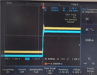
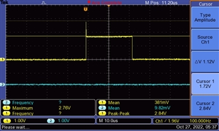
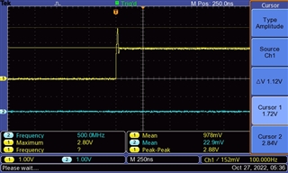
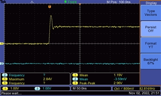
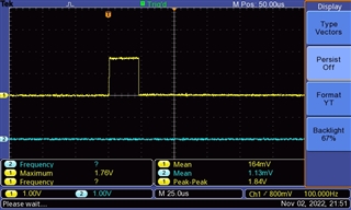
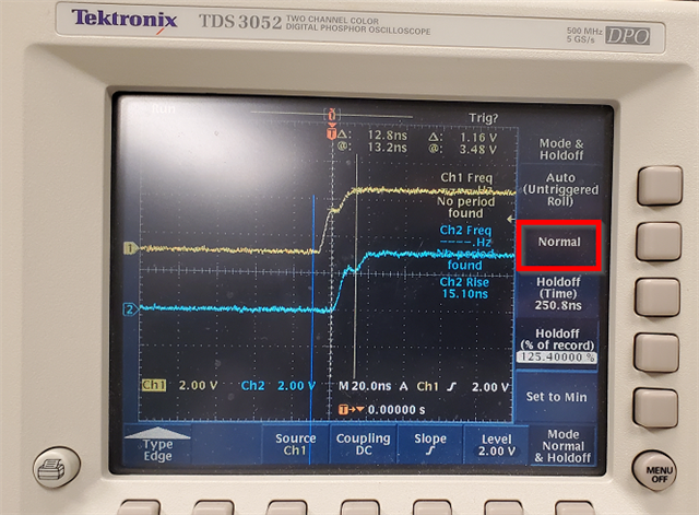
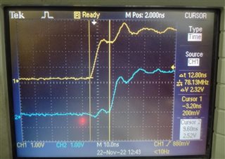
    I would also like to know if the reference validation remains relevant for the DPLL reference validation settings for the 100 Hz reference in use. The On duration is 20 us; Peak overshoot voltage - 2.84 V and High voltage of 1.8 V. The oscilloscope images are attached.

  • Hi Akanksh,

    Let me clarify my previous post and your questions:

    1. Can you try routing 12.8 MHz from a signal generator into the XO_P input of the LMK05318BEVM? That is what I used to confirm this configuration.
    2. We do not recommend using a 10 MHz XO input frequency to ensure there is a fractional relationship between the XO and the BAW VCO (2500 MHz).
    3. No, the LMK05318B does not accept crystal inputs into the XO pin; therefore, you cannot test with the 12 MHz crystal.
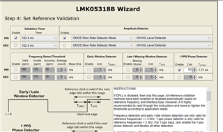
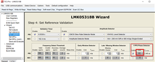
    4. When using low frequency signals (< 2kHz), the device must use the 1-PPS configuration. In that case, the PRIREF_PH_VALID_THR value (see image below) determines the XO accuracy.
      1. If the PRIREF_PH_VALID_THR = 63 and XO frequency = 12.8 MHz, then the required XO accuracy is ± 63/12.8 = ± 4.92 ppm. 
      2. If the PRIREF_PH_VALID_THR = 63 and XO frequency = 48.0048 MHz, then the required XO accuracy is ± 63/48.0048 = ± 1.31 ppm. 
        1. The on-board 48.0048 MHz XO has a ± 20 ppm accuracy which is why it will not be possible to generate a locking config for such oscillator.
      3. We recommend using the 12.8 MHz XO frequency because the accuracy requirement is larger than the 48.0048 MHz.
    5. Yes, the reference validation is still valid for 100 Hz input. 
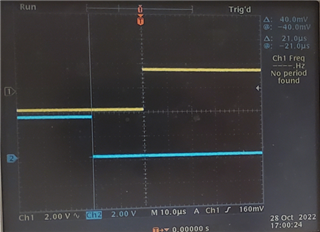
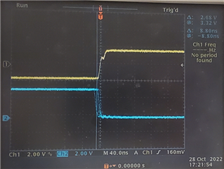
    6. The DPLL R divider output is sourced from the DPLL reference (100 Hz input). The DPLL FB divider is sourced from the VCO output (2500 MHz). When the DPLL is locked, these two outputs should be 0deg in-phase or 180deg out of phase. If you bring these two signals out through STATx and connect them to the oscilloscope, you can confirm whether the DPLL is actually locked. If the waveforms drift from each other, then the DPLL is not locked. Because the DPLL LBW is set to 0.1 Hz, it will take longer for the DPLL to lock. The pictures below demonstrate the gradual phase alignment between the two signals.
      1. After several minutes, the DPLL R divider and DPLL FB divider waveforms are 21 us apart.
      2. Two minutes after the above time, the waveforms are 2.6 us apart. The DPLL FB divider output continues to "inch" towards the DPLL R divider as the DPLL settings update to attain lock to the reference.
      3. After about 20 minutes, the DPLL locks (DPLL_LOPL = 0).

    Regards,

    Jennifer

  • Hi Jennifer,

    We are trying the 26 MHz Oscillator, 0.5 ppm accuracy as of now due to non-availability of clock generator. As per the calculation for required XO accuracy it is within the limit. Hence is it okay to use this clock for the configuration file shared? After the DPLL script, on checking the status, the HLDOVR_INTR flag is set as high and the DPLL's Active reference goes into Holdover. The R divider and FB divider voltages are displayed as high throughout. Is it due to the reference signal issue?

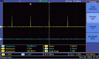
    The plot of the 100 Hz clock( which will be used in the final application) generated from a generic chip is as follows:

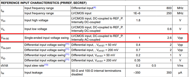
    a. Since the peak voltage goes ~ 3V is it causing issues in reference locking? Since the table from the datasheet shows max of 2.6 Vpp. 

    b. ON period for the signal is ~ 22us.

    c. Time period is constant at 10ms.

    Regards

    Akanksh S

  • Hi Jennifer,

    The output to output phase lock is seen on our device for APLL1 output, as shown in the plots shared on Oct 22. But our requirement is phase locking between PRI_REF signal and the outputs of frequency 6.912 MHz and 30.72 MHz which we are not able to observe in our setup. Can you confirm if the phase lock is possible with the above scenario?

  • Hi Akanksh,

    Yes it is possible for outputs to lock to 100 Hz PRIREF but for XO = 26 MHz, I will need to generate another config. This I can provide next week.

    Regards,

    Jennifer

  • Hi Jennifer,

    I got the clock generator to generate the 12.8 MHz output. The output locking to input doesn't occur even after 20 minutes for the configuration file shared ("e2e LMK05318B_XO=12.8 MHz_PRIREF=100Hz_OUT=30.72 and 6.912 MHz_Oct 21 2022.tcs"). Should the SYNC_SW be checked throughout or just an assert and de-assert within 5 seconds is sufficient? The holdover issue of the DPLL PRI_REF seems to be resolved with a proper 100 Hz clock, but the Output clock locking to input is still not possible. Should the "Frequency Plan" be manually selected in the "Set output section" to avoid APLL2 P2 post divider?

    On trying a different scenario: The EVM default configuration file with 12.8 MHz XO changed(Keeping other parameters constant), the output lock with the input is observed with the PRI_REF(25MHz).  

  • Hi Jennifer.

    We could able to lock PRIREF to O/P clocks using APLL1. But still with APLL2, we are unable to lock.

    Test Details and O/P frequencies for which we achieved phase lock

    1.)

    XO frequency = 12.8MHz

    PRIREF frequency = 100Hz

    O/P clock1 frequency = 6.25MHz

    O/P clock2 frequency = 31.25MHz

    2.)

    XO frequency = 12.8MHz

    PRIREF frequency = 100Hz

    O/P clock1 frequency = 6.25MHz

    O/P clock2 frequency = 25MHz

    But we are not able to phase lock for our expected freqs : 30.72MHz and 6.912MHz either by using APLL1 or APLL2.

    Please send us the configuration file which phase locks for our expected frequencies at the earliest.

    Customer is unable to move forward as he is waiting for phase lock of expected freqs.


  • Hi Jennifer,

    Is there any specific duty cycle and rise time requirement of the PRI_REF signal in order to lock the reference and prevent the board from going into holdover?

  • Hi Akanksh,

    1. I got the clock generator to generate the 12.8 MHz output. The output locking to input doesn't occur even after 20 minutes for the configuration file shared ("e2e LMK05318B_XO=12.8 MHz_PRIREF=100Hz_OUT=30.72 and 6.912 MHz_Oct 21 2022.tcs"). 
      1. Please elaborate further on "output locking to input doesn't occur" by answering below:
        1. What is the LOPL_DPLL and LOFL_DPLL status signal?
        2. Please have customer route DPLL R divider and DPLL FB divider to STATx pins. Connect these two signals to the scope and share the screen captures as I mentioned previously.
        3. Do you see the two waveforms drifting (scope can't trigger to both)?
        4. Checking these two waveforms is imperative to determine whether the DPLL is actually not phase locking or it is a problem with the device not reporting DPLL lock. If it's a problem with reporting, the reference validation settings need to be adjusted.
        5. I set a timer and it took about 50 minutes for the LOPL_DPLL status bit to clear.
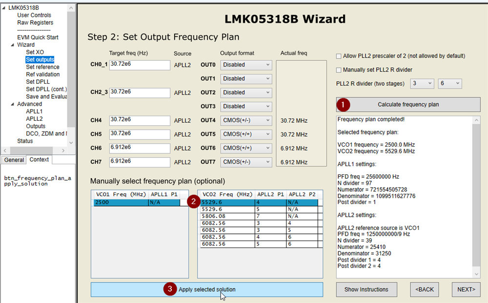
    2. Should the "Frequency Plan" be manually selected in the "Set output section" to avoid APLL2 P2 post divider?
      1. Yes, you can manually set the VCO to avoid APLL2 P2 post divider. 
      2. After clicking "Calculate Frequency Plan", choose the desired VCO from the "Manually Select Frequency Plan" section, and select "Apply Selected Solution".
      3. I've attached a new config where only APLL2 P1 is used.
      4. e2e LMK05318B_XO=12.8 MHz_PRIREF=100Hz_OUT=30.72 and 6.912 MHz_Nov 15 2022.tcs
    3. Should the SYNC_SW be checked throughout or just an assert and de-assert within 5 seconds is sufficient?
      1. SYNC_SW (the global SYNC enable) should be checked when you want to assert SYNC. 
      2. Outputs or PLLs with the SYNC enabled (CHn_SYNC_EN or PLLn_Pn_SYNC_EN) are muted when SYNC_SW = 1. Note that if SYNC_SW is checked prior to setting these enable bits, then the SYNC will not take place. In this case, you will have to issue a toggle (101)
      3. After de-asserting SYNC (SYNC_SW = 0), the sync'ed outputs are unmuted and phase-aligned.
    4. Is there any specific duty cycle and rise time requirement of the PRI_REF signal in order to lock the reference and prevent the board from going into holdover?
      1. The PRIREF/SECREF inputs use edge detection to validate and are not based on the duty cycle.
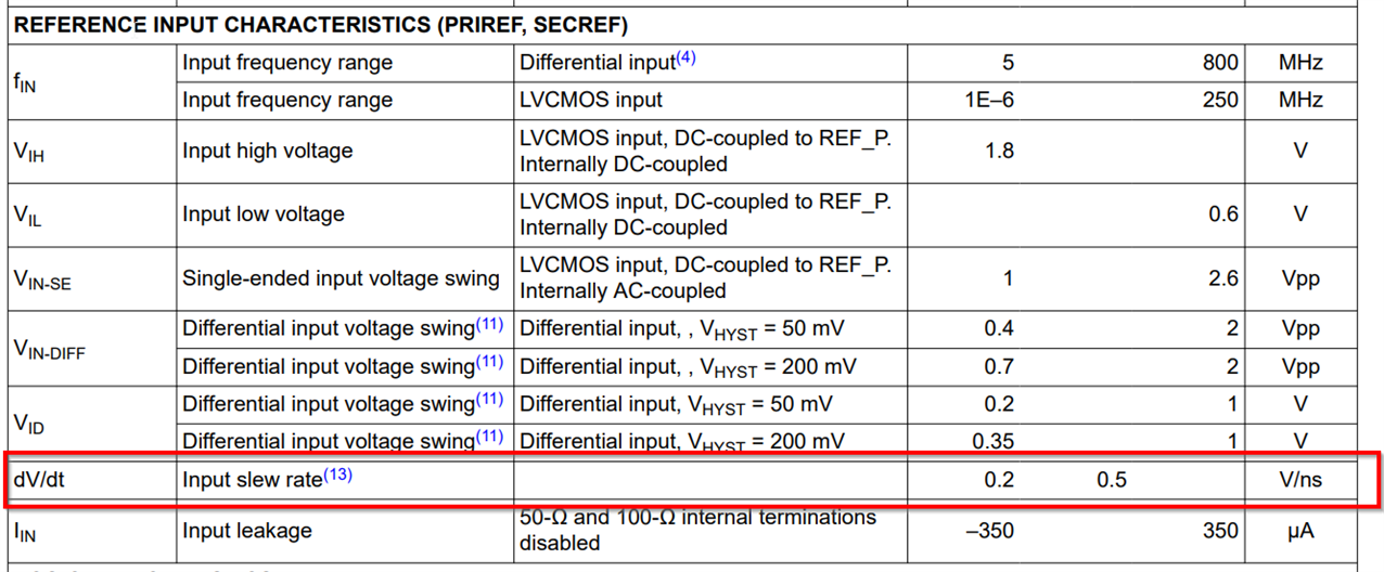
      2. The rise time requirements are specified by the slew rate noted in the datasheet:
  • Hi Jennifer,

    The LOPL_DPLL is cleared after 50 minutes on our setup too, but the LOFL_DPLL continues to remain asserted while status is read after clearing all the flags. What could be the possible issue for this?

  • Hi Akanksh,

    Good to hear the LOPL_DPLL does clear. Due to a lower DPLL LBW (0.01 Hz), the time it takes to phase lock (and report it) is much longer.

    I also have similar symptoms where LOFL_DPLL toggles continuously. This is something I'm still investigating as it is a matter of the device not properly reporting DPLL Frequency Lock Detect and not actually a matter of the DPLL not frequency locking. If LOPL_DPLL = 0, the DPLL is locked.

    Regards,

    Jennifer

  • Akanksh, Gurunath,

    From our Nov 17 call, you requested configs for PRIREF = 1 Hz, 10 Hz, and 1 MHz to output 6.912 MHz and 30.72 MHz. 

    Today, I can provide the following configs:

    I've confirmed DPLL lock through the Status page and DPLL R & FB divider. as well as confirmed the frequencies are as expected on a frequency counter.

    Please let me know if you have success attaining continuous DPLL lock with these configs.

    Regards,

    Jennifer

  • Hi Jennifer,

    We tried the configs shared and the observations are as follows:

    • PRIREF = 1 MHz(previously 1 Hz or 1PPS) 
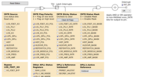
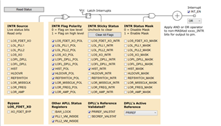
      • The LOPL and LOFL flags are unchecked but the HIST_INTR flag is asserted. Could you explain what does this flag signify?
      • The R divider waveform and the FB divider remain to be locked.
      • The PRI_REF to OUTPUT clock still remain unlocked.
    • PRIREF = 1 pps(previously 1 MHz)
      • The LOPL and LOFL flags are asserted in this scenario.
      • The FB divider waveform drifts away from the R divider waveform which is triggered signal.
      • The PRI_REF to OUTPUT clock still remain unlocked.

    EDIT: Typo error in the last message for the PRI_REF is highlighted.

  • Akanksh,

    Some comments and questions:

    • Regarding PRIREF = 1 Hz/PPS config
      • HIST_INTR is the interrupt flag for the tuning word history update of the DPLL. Please refer to Section 9.3.7.4 of the datasheet for additional details on how this gets set. This bit does not indicate a lock status. Note that interrupt flags must be manually cleared. 
      • What do you mean "remain to be locked" for the DPLL R and FB dividers? Were you able to lock?
        • On my bench, I observe the FB divider moves around (about +/- 10 ns) the PRIREF-- such drifting around the input is expected as the DPLL updates.
        • The DPLL FB divider is sourced from the VCO output. This FB divider represents the OUT signal because after the VCO output, there is only the PLL Pn divider and output channel dividers. This means that if there is lock on the DPLL R and FB dividers, there should be lock on the PRIREF and outputs. 
      • How are you defining PRIREF and outputs are "not locked"?
      • Could be a triggering issue? You can try setting it to "Normal" mode if you have this option on the scope. 
      • How are you sourcing the 1 Hz? Please provide a part number.
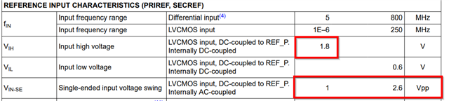
      • What is the signal level of this input? Please make sure inputs are within the spec. Single-ended inputs should be 1-2.6 Vpp. 
      • Is PRIREF_VALSTAT =1?
    • Regarding PRIREF = 1 MHz config
      • How are you sourcing the 1 MHz? Please provide a part number.
      • What is the signal level of this input? Please make sure inputs are within the spec.
      • Is PRIREF_VALSTAT =1?

    Regards,

    Jennifer

  • Hi Jennifer,

    Following are my response to the questions:

    1. For PRI_REF = 1 MHz( typo error in the previous response as 1pps)

    Note that interrupt flags must be manually cleared.

    Yes I have selected the " Clear All Flags" and obtained the flag status by clicking "Read status" option.

    What do you mean "remain to be locked" for the DPLL R and FB dividers? Were you able to lock

    The R and FB divider are apart by 13 ns in my case. The plot is as follows:

    "Remain to be locked" meant that the above waveforms do not drift apart from each other and the Δt is within 10 ns to 14 ns.

    The DPLL FB divider is sourced from the VCO output. This FB divider represents the OUT signal because after the VCO output, there is only the PLL Pn divider and output channel dividers. This means that if there is lock on the DPLL R and FB dividers, there should be lock on the PRIREF and outputs. 

    But considering our Output frequencies of 6.912 MHz and 30.72 MHz they are derived from the VCO2 output.

    How are you defining PRIREF and outputs are "not locked"?

    We set the PRI_REF signal triggered source(CH1) and the CH2 is connected to the OUT7_P of the EVAL board. The lock between two signals is confirmed when the rising edge of PRI_REF is aligned to the rising edge of OUT7_P signal. The channel 2 remains unlocked to the triggered source(video file attached).

    The output locked to input as observed for CH7_P APLL1 output of 25 MHz( on CH2) and PRI_REF 1 MHz(on CH1), with the same configuration file shared:

    Could be a triggering issue? You can try setting it to "Normal" mode if you have this option on the scope

    Yes the Mode is set as "Normal" mode in the trigger menu.

    How are you sourcing the 1 Hz? Please provide a part number.

    The source for 1 MHz and 1 Hz PRI_REF clock is from CG635 synthesised clock generator, CMOS 1.8V output.

    Is PRIREF_VALSTAT =1?

    Yes, PRIREF_VALSTAT=1.


    Regarding PRIREF = 1 MHz config

    This is the response related to 1 PPS as PRIREF( mentioned as 1 MHz before due to typo error).

    How are you sourcing the 1 MHz? Please provide a part number.

    The source for 1 MHz PRI_REF clock is from CG635 synthesised clock generator.

    What is the signal level of this input? Please make sure inputs are within the spec

    Signal level is 1.8V DC.

    Is PRIREF_VALSTAT =1?

    Yes, PRIREF_VALSTAT = 1. 

    Is it able to obtain lock of reference to output for the 10 Hz reference input. Can you share the config file if possible?

  • Hi Akanksh,

    Because of the Thanksgiving holiday in the U.S., TI E2E design support forum responses may be delayed the week of Nov. 21. Thank you for your patience.

    regards,

    Julian

  • Hi Jennifer,

    As per the data sheet, the information regarding phase alignment. The Outputs phase alignment is also not seen after a 0 -> 1  -> 0 toggle of SYNC_SW. What could be the possible cause for this issue?


  • Hi Akanksh,

    Let's hop on another call to discuss as it will help clear misunderstandings on my end. I'll send an email, see if you can make it. There is some discrepancy between "locking" and absolute phase alignment. I think you may want the zero-delay mode feature. 

    Regards,

    Jennifer

  • Hi Akanksh,

    These are the next steps from our call:

    1. Ensure SMA connections are properly tightened (loose connections can cause phase hits).
    2. Ensure PRIREF input meets the datasheet requirements of a min VIH = 1.8 V and has a swing between 1-2.6 Vpp. The input I use is 2.65 V LVCMOS.
    3. Try a different 12.8 MHz XO input source such as a signal generator.
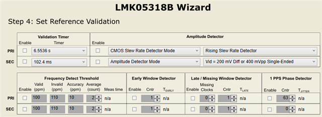
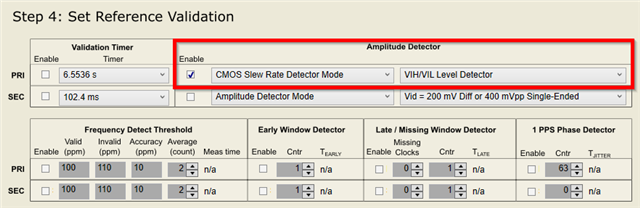
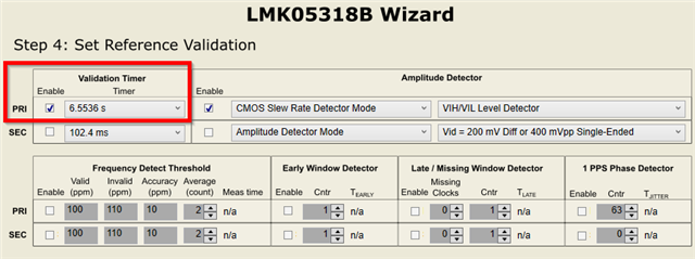
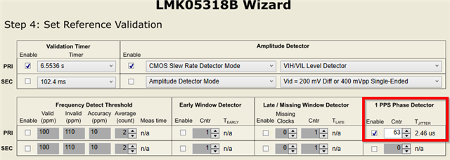
    4. Ensure PRIREF_VALSTAT = 1 before debugging LOPL_DPLL and LOFL_DPLL. Enable the validation detectors in the following order:
      1. Uncheck all Reference Validations. You should see PRIREF_VALSTAT = 1.
      2. Enable Amplitude Detector with settings CMOS Slew Rate Detector Mode and VIH/VIL Level Detector. If the input meets the required swing and VIH/VIL levels, you should see PRIREF_VALSTAT = 1.
      3. Enable Validation Timer. If the input stays valid for the specified time, it will report PRIREF_VALSTAT = 1. In this state, the amplitude detector must be valid for ~6 s to report valid.
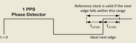
      4. Enable 1 PPS Phase Detector. Note that in our call I said to increase the 1 PPS Detector--this is incorrect because the counter is already at the maximum value (63) for maximum jitter allowance. If the 1 PPS edge is being detected within the allotted jitter allowance, PRIREF_VALSTAT = 1.
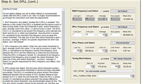
    5. Modify the LOPL and LOFL thresholds.
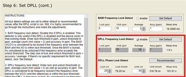
      1. Increase the LOPL parameters all the way until you always get LOPL = 0. Once such state is reached, start decreasing right before LOPL = 1. Note that LOFL and LOPL lock & unlock thresholds should maintain the same difference. For example, for the DPLL phase lock detect, lock = 28 and unlock 30. If you increase the lock by 4, the unlock should also increase by 4.

    Regards,

    Jennifer

  • Hi Jennifer,

    We could generate the phase locking of the input to output clock for the 1-pps clock reference(from CG635) based on the procedure discussed over the meeting. 

    Now, our requirement is to lock to a 1-pps clock generated from our custom chip which has a maximum possible time period variation of 1±0.00474 seconds, hence the corresponding variation in frequency is observed on the frequency counter too. On using this clock as the reference, the PRIREF is selected for ~5 seconds and remains unlocked for next 5 seconds.

    Here the  PRIREF_VALSTAT = 1 is ensured always till 4.c mentioned in the previous reply.

    Enable Validation Timer. If the input stays valid for the specified time, it will report PRIREF_VALSTAT = 1. In this state, the amplitude detector must be valid for ~6 s to report valid

    On enabling the 1-pps phase detector, the DPLL Reference keeps switching from PRIREF to Holdover.

    Since PRIREF_VALSTAT = 1 is not ensured, I didn't try modifying the LOPL and LOFL thresholds.


  • Hi Jennifer,

    We need support on getting the proper DPLL LBW changes and the corresponding config file for PRIREF = 9.9338 Hz. For this frequency, we are able to keep the PRIREF_VALSTAT = 1 always( jitter tolerance within 0.5us) hence is it possible to use this as specific Reference frequency. 

    Tried the following with the 1 Hz config file(LMK05318B_XO=12.8 MHz_PRIREF=1PPS_OUT=30.72 and 6.912 MHz_Nov 18 2022.tcs) with changes on PRIREF:

    1.For LBW=0.1 Hz, the R-divider and FB-Divider never locks and drifts apart very fast. 

    2. For LBW = 0.01 Hz( same as the 1 Hz config) the R and FB remain apart by 2us even after 30 minutes of observation.

    Regards

    Akanksh S

  • Hi Jennifer,

    Are there any possible solution on using the PRIREF frequency of 9.9338 Hz and the possible LBW frequency that can be tuned for best performance and faster locking. 

    Regards

    Akanksh

  • Hello Akanksh,

    We will get back to you in the next few days. Sorry for the delay.

    Best,

    Andrea

  • Hi Jennifer/Andrea,

    Any update on locking the DPLL with the fractional Reference frequency and the LBW to be used. I am able to get a considerable frequency lock at output. The R divider and FB divider remains at an offset of 200 to 300 ns even upon monitoring for ~ 1 hour. The configuration file I have used is attached.LMK_9.933755Hz_Working_20221216.tcs

  • Hi Akanksh,

    Apologize for the delay. 

    Slow lock times are expected for such low DPLL LBW frequencies (which are required for low frequencies such as ~10 Hz).

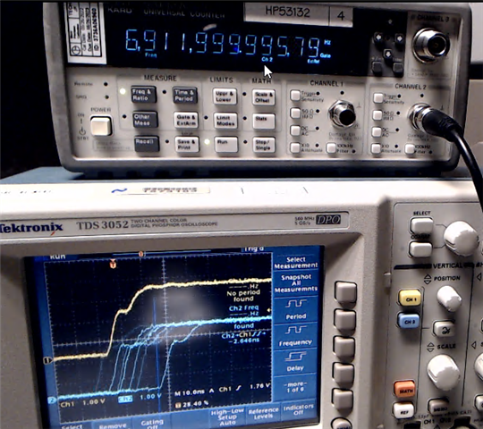
    I tested your config yesterday and attained LOPL=0 after ~1 hour but LOFL toggled. On the scope, it was clear the frequency and phase was locked (6.912 MHz within <1 ppm error). I left the setup running overnight, untouched. Today, I checked the outputs are still locked, LOPL=0 (LOPL interrupt flag didn't get set either) but LOFL continues to toggle. This comes to be an issue with the LOFL reporting and getting triggered incorrectly.

    Looking at the DPLL register settings in detail, I find that the frequency lock timer values are properly calculated.

    It continues to remain unclear why the DPLL is reporting LOFL. I will need to discuss with design for further insight.

    Regards,

    Jennifer

  • Note: We have continued this thread offline.