This thread has been locked.

If you have a related question, please click the "Ask a related question" button in the top right corner. The newly created question will be automatically linked to this question.

LMK04828: DAC3XJ8XEVM : PLL2 NOT Locking for 100MHz LVPECL

Part Number: LMK04828

Hi,

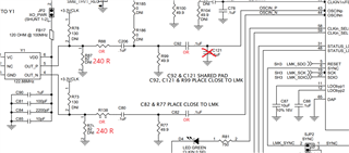
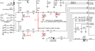
We are using DAC3XJ8XEVM EVAL Board which default comes with 122.28MHz LVCMOS to OSCIN.

DAC3XJ8XEVM-SCH_D.pdf

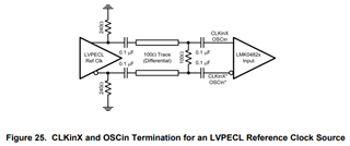
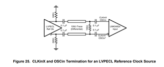
We are changing the Y1 to 100MHz LVPECL https://www.crystek.com/crystal/spec-sheets/vcxo/CVPD-922.pdf  and followed LVPECL Input circuit to OSC IN Input

But the PLL2 is not locking.

With external Input to J17 CLKIN1 PLL1 is locking but PLL2 is not locking 

Anything we are missing..?

  • Hello Lakshminarayana,

    There are two main things I noticed that could cause the PLL2 not to lock. First off, if you are using the software provided by TI to run the evaluation board, it won't work since its programmed for a 122.28 MHz signal. Secondly, and most importantly, the main problem is that the DAC3XJ8XEVM is programmed for a CMOS input, as you mentioned, which is a single-ended input. If you look at the block diagram you provided, Y1 positive's pin is not populated, hence no signal is going through that pin. Therefore, when you use an LVPECL signal that is differential, not the entire signal is passed into the LMK04828, leading to PLL2 not locking. I have attached a design suggestion to fix this issue and populate that pin correctly from Y1.

    Also, PLL1 locking is independent of PLL2 locking, it is mainly dependent on the reference input signal, and not the VCXO you are using.

    If this has not answered your question/solved your problem, please in your response attach a screenshot or file of your DAC3XJ8X GUI and/or your desired output frequencies.

    Good Luck,

    Andrea

  • Therefore, when you use an LVPECL signal that is differential, not the entire signal is passed into the LMK04828, leading to PLL2 not locking. I have attached a design suggestion to fix this issue and populate that pin correctly from Y1.

    Yes, we have tried with Differential Input termination to LMK as below, Though PLL is not locking.

    First off, if you are using the software provided by TI to run the evaluation board, it won't work since its programmed for a 122.28 MHz signal

    We have tried changing the Divider values for 100MHz, Still PLL2 doesn't lock.

    In GUI is there an option to select for OSCIN single (CMOS) or Differential Input with bipolar ?

    Anything else we are missing.

  • Hi Lakshminarayana,

    For the LVPECL differential input, OSCin input termination should be suggested to have 100ohm differentially. Here, you can provide the 100ohm resistor across the differential line and see the performance.

    Apart from this, with the change of VCXO, you could probably tune the PLL2 loop filter and you can use the PLLatinum sim tool for loop filter simulation.

    The change of the input termination for the OSCin would be sufficient for different input format signals (single ended or differential).

    Thanks!

    Regards,

    Ajeet Pal