This thread has been locked.

If you have a related question, please click the "Ask a related question" button in the top right corner. The newly created question will be automatically linked to this question.

LMK04228: LMK04228 as a reference clock design

Part Number: LMK04228
Other Parts Discussed in Thread: LMK04828

Hello, I have been debugging a board card which uses lmk04228 as the reference clock of optical fiber communication.

Problem1: The output clock of lmk04228 is 100m, and the input crystal oscillator is also used as a reference. It is found that the output frequency of one board card is only 99m, which is smaller than the output of other boards. We are also eliminating hardware problems, and we hope that you can help us check whether there is any problem with the configuration

Problem 2, there are two pieces of the board of the clock output is normal, but still can't normal communication optical transceiver, tried to add a heat sink, or after an insulating sheet metal press on a chip, optical transceiver can work normally, observe the oscilloscope and jitter output clock without any change, so don't know what is the interference

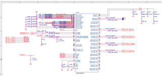
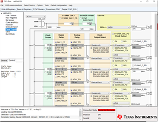
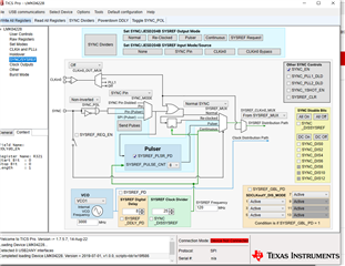
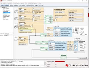
The following is our configuration and schematic diagram, please help to check whether there is any problem in the design

  • The frequency deviation of one card is only about 0.5mhz, which seems not to have a great impact on the current test. Is the output frequency deviation of different lmk04228 new products normal? Mainly focused on problem 2, my optical transceiver can only work properly by pressing the clock chip with an insulated back metal sheet. Is this effect caused by configuration or is there a problem with our pcb design

  • Hi,

    LMK04228 can be used as jitter cleaner in dual PLL mode or clock generator in single PLL mode (PLL2) or in distribution mode.

    In any of the PLL mode, it would need an external VCXO at OSCin input, which would be oscillator for PLL1 and/or input to the PLL2.

    Based on your schematic / hardware, you doesn't have VCXO at OSCin input. Hence you can't be use the device in PLL mode. 

    If your input and output frequency be 100MHz, you can use it in distribution mode with the input at CLKin1 port and get the bypassed output at DCLKout/SDCLKout channels.

    Thanks!

    Regards,
    Ajeet Pal 

  • I see that the manual of lmk04228 does not support the distribution mode, is it possible to use the distribution mode for lmk04828

  • I tried to use the distribution mode on the development board and it worked I'll try it on our own card. Thank you

  • Hi,

    Apologies for the confusion. There is an correction in the previous reply, where the distribution mode is supported by LMK04828 not LMK04228. If you might be getting it worked (LMK04228) in distribution mode, it may not be reliable. Hence, you need to use it in PLL mode only. Otherwise, you can replace with LMK04828 and use in distribution mode in the existing hardware.

    Thanks!

    Regards,
    Ajeet Pal

    • Thank you for your help. The distribution mode can be used normally,

      NowI have some questions:

      1   clkin0/clkin1 as an external input clock through pll1 and pll2 can the output clock and clkin0/clkin1 keep synchronization or there is only a certain phase relationship
    • 2  Whether osc in must be connected to crystal oscillator to use pll1 and pll2 ?
  • Hi,

    1   clkin0/clkin1 as an external input clock through pll1 and pll2 can the output clock and clkin0/clkin1 keep synchronization or there is only a certain phase relationship

    LMK04228 doesn't support the 0-delay mode / feedback mux, hence when used the channel dividers, it can't meet the phase deterministic between input and the outputs. Phase relationship can be maintained for divider bypass.

    2  Whether osc in must be connected to crystal oscillator to use pll1 and pll2 ?

    Yes, external VCXO / crystal oscillator must be connected at OSCin to operate the device in dual PLL and/or single PLL mode (PLL2 only) respectively.

    Thanks!

    Regards,

    Ajeet Pal