


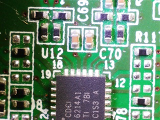
Part Number: CDCI6214
Other Parts Discussed in Thread: CDCE6214
This goes for both CDCE6214 and CDCI6214.
Assuming REFSEL = HIGH and PRIREF_P/N is our Input using LVCMOS input clock.
Can you confirm the below please?
1) The PRIREF_N should be connected directly to GND? Or should it be pulled-down through a resistor? Recommended value...?
2) The SECREF is unused, and so both SECREF_P/N pins should be left floating. Yes?
3) For CDCI6214 we want the HCSL 50Ω termination resistors as close to the 33Ω resistors as possible, right?
I ask because that is how they were designed in our AM65xx PCIe reference design.TMDX654GPEVM 1L PCIe / USB3.1 PCB Layout
Regards,
Darren

