This thread has been locked.

If you have a related question, please click the "Ask a related question" button in the top right corner. The newly created question will be automatically linked to this question.

LMK04828: ±1 VCO cycle error for LMKs' output device clock aligning when performing multiple-LMK synchronization

Part Number: LMK04828

Hi there,

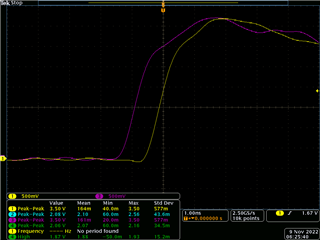
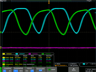
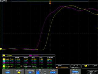
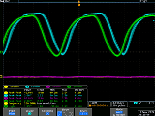
I have two LMK04828 to be synchronized. However, I get ±1 VCO cycle error for LMKs' output device clock (DCLKout2) aligning after power-cycle. 

I didn't use any PLL on LMK04828. Therefore, only divider reset was involved in the synchronization.

The external 1GHz clock is distributed to CLKin1 port on LMKs with the same path length.

The SYNC was performed by toggling SYNC pins on LMKs simultaneously with identical length.

For SYNC operation, I used normal SYNC mode. For SYSREF operation, I used SYSREF pulser mode.

The following is my register config:

(0x0000,0x90)
(0x0000,0x10)
(0x0000,0x10)
(0x0100,0x61)
(0x0101,0x22)
(0x0103,0x02)
(0x0104,0x20)
(0x0106,0xf0)
(0x0107,0x55)
(0x0108,0x64)
(0x0109,0x22)
(0x010b,0x07)
(0x010c,0x20)
(0x010e,0x80)
(0x010f,0x11)
(0x0110,0x61)
(0x0111,0x22)
(0x0113,0x02)
(0x0114,0x20)
(0x0116,0xf0)
(0x0117,0x57)
(0x0118,0x61)
(0x0119,0x22)
(0x011b,0x02)
(0x011c,0x20)
(0x011e,0xf0)
(0x011f,0x57)
(0x0120,0x62)
(0x0121,0x22)
(0x0123,0x05)
(0x0124,0x20)
(0x0126,0xb0)
(0x0127,0x11)
(0x0128,0x68)
(0x0129,0x22)
(0x012c,0x20)
(0x012e,0xf7)
(0x012f,0x01)
(0x0130,0x61)
(0x0133,0x02)
(0x0134,0x20)
(0x0136,0xf7)
(0x0138,0x40)
(0x0139,0x00)
(0x013a,0x01)
(0x013b,0x00)
(0x013c,0x00)
(0x013d,0x08)
(0x013e,0x02)
(0x0140,0xf0)
(0x0143,0x91)
(0x0143,0x91)
(0x0143,0x11)
(0x0144,0x49)
(0x0145,0x7f)
(0x0146,0x00)
(0x0147,0x10)
(0x0148,0x33)
(0x0149,0x40)
(0x014a,0x02)
(0x014b,0x05)
(0x014c,0xff)
(0x0150,0x00)
(0x0156,0x78)
(0x015f,0x0b)
(0x0161,0x01)
(0x0162,0x44)
(0x016e,0x13)
(0x0171,0xaa)
(0x0172,0x02)
(0x0173,0x60)
(0x017c,0x15)
(0x017d,0x33)
(0x1ffd,0x00)
(0x1ffe,0x00)
(0x1fff,0x53)
Toggle SYNC pins on LMKs simultaneously
(0x0144,0xff)
(0x0143,0x12)
(0x0139,0x02)

My question is that whether ±1 VCO cycle error is expected to happen for LMKs' output device clock aligning? Did I miss anything to synchronize the LMKs? Shall I use zero-delay mode to get rid of the VCO cycle error?

Thanks and best,

Yilun

  • Hi Yilun,

    Your register settings look good, except SYNC operation. How are you toggling the SYNC pin? can you able to probe the SYNC input (pulse) at both LMKs SYNC pin? Both device should see the SYNC raising edge at the same time and it will reset the dividers with the SYNC raising edge input.

    Thanks!

    Regards,
    Ajeet Pal

  • Hi Ajeet,

    For the SYNC pin toggling, I have a register called "lmksync" in the Verilog top level.

    assign hw.fmc1.lmk_sync=lbreg.lmksync;
    assign hw.fmc2.lmk_sync=lbreg.lmksync;

    The "hw.fmc1.lmk_sync" and "hw.fmc2.lmk_sync" are connected to FPGA pins respectively through OBUFs. The corresponding FPGA pins are connected to the LMK04828 SYNC pins via FMC connectors.

    The "lbreg.lmksync" can be accessed by writing ethernet register map.

    regmap.write((('lmksync',1),))
    regmap.write((('lmksync',0),))

    I have probed the LMK04828 SYNC pins and seen the SYNC rising edge (left fig below). The right figure below is the DCLKout2 from the two LMK ICs.

    I also have another "+1 VCO cycle error" probe results shown below.

    It seems that there is a 800ps difference of the two SYNC rising edges. But the difference is deterministic and constant between "+0 VCO cycle error" and "+1 VCO cycle error". Even though there is 800 ps difference of two SYNC signals, the deterministic difference will not lead to the two patterns of DCLKout2? Am I understanding correctly?

    For the register 0x143 bit 6 (SYNC_1SHOT_EN) of LMK04828, I set it to 0 (which means "SYNC is level sensitive and outputs are held in SYNC while SYNC is asserted"). How do we understand the level sensitive?

    Looking forward to your reply.

    Thanks and best,

    Yilun

  • Hi Yilun,

    The output divider reset for multi device can be performed through external sync input at SYNC pin or CLKin0 pins. The input sync signal must be re-timed to the VCO cycle / distribution clock cycle for phased aligned reset. Hence the input sync signal should meet the setup time requirement. Also the delay in the sync input may not be exact same at the divider output, as it is re-timing with the clock cycle.

    But due to the CMOS variability in the SYNC pin path, there is 3-5ns uncertainty in the sync pin timing, which makes SYNCing output dividers through SYNC pin almost impossible at 1GHz clock input, whose clock cycle period 1ns. that's will provide the multiple VCO cycle error. 

    Whereas the sync through CLKin0 input pin has precise setup timing (≤ 150ps) and should be possible phase aligned divider reset. but need to have rising edge aligned synced inputs to multiple devices.

    Thanks!

    Regards,
    Ajeet Pal 

  • Hi Ajeet,

    I tried performing external sync at CLKin0 pins. It seems that I got more output patterns of DCLKout2 (more than ±1 VCO cycle error).

    The sync toggling was sent through "lbreg.lmksync", which was connected to differential FPGA pins with OBUFDS. 

    assign hw.fmc1.lmk_clkin0=lbreg.lmksync;
    assign hw.fmc2.lmk_clkin0=lbreg.lmksync;

    Then the FPGA pins were directly connected to LMK CLKin0(*) pins.

    Here are my register settings:

    (0x0000,0x90)
    (0x0000,0x10)
    (0x0000,0x10)
    (0x0100,0x61)
    (0x0101,0x22)
    (0x0103,0x02)
    (0x0104,0x20)
    (0x0106,0xf0)
    (0x0107,0x55)
    (0x0108,0x64)
    (0x0109,0x22)
    (0x010b,0x07)
    (0x010c,0x20)
    (0x010e,0x80)
    (0x010f,0x11)
    (0x0110,0x61)
    (0x0111,0x22)
    (0x0113,0x02)
    (0x0114,0x20)
    (0x0116,0xf0)
    (0x0117,0x57)
    (0x0118,0x61)
    (0x0119,0x22)
    (0x011b,0x02)
    (0x011c,0x20)
    (0x011e,0xf0)
    (0x011f,0x57)
    (0x0120,0x62)
    (0x0121,0x22)
    (0x0123,0x05)
    (0x0124,0x20)
    (0x0126,0xb0)
    (0x0127,0x11)
    (0x0128,0x68)
    (0x0129,0x22)
    (0x012c,0x20)
    (0x012e,0xf7)
    (0x012f,0x01)
    (0x0130,0x61)
    (0x0133,0x02)
    (0x0134,0x20)
    (0x0136,0xf7)
    (0x0138,0x40)
    (0x0139,0x00)
    (0x013a,0x01)
    (0x013b,0x00)
    (0x013c,0x00)
    (0x013d,0x08)
    (0x013e,0x02)
    (0x0140,0xf0)
    (0x0143,0x91)
    (0x0143,0x91)
    (0x0143,0x11)
    (0x0144,0x49)
    (0x0145,0x7f)
    (0x0146,0x00)
    (0x0147,0x10)
    (0x0148,0x33)
    (0x0149,0x40)
    (0x014a,0x02)
    (0x014b,0x05)
    (0x014c,0xff)
    (0x0150,0x00)
    (0x0156,0x78)
    (0x015f,0x0b)
    (0x0161,0x01)
    (0x0162,0x44)
    (0x016e,0x13)
    (0x0171,0xaa)
    (0x0172,0x02)
    (0x0173,0x60)
    (0x017c,0x15)
    (0x017d,0x33)
    (0x1ffd,0x00)
    (0x1ffe,0x00)
    (0x1fff,0x53)
    Toggle CLKin0 on LMKs simultaneously
    (0x0144,0xff)
    (0x0143,0x12)
    (0x0139,0x03)

    What am I missing in the register setting or the hardware setup?

    Thanks and best,

    Yilun

  • Hi Yilun,

    For external SYNC at CLKin0 (precise setup timing), the input signal should be DC coupled differential and should meet the digital logic level for resetting the dividers.

    Register config looks good and seems HW setup need to be updated for SYNC as well as SYNC input to both devices should be aligned.

    Thanks!

    Regards,
    Ajeet Pal

  • Hi Ajeet,

    The CLKin0 pin is connected to the FPGA pins directly, which is LVCOMS18 I/O standard (1.8V). It seems that it doesn't meet the V_CLKin0 high input voltage requirement (>2.0V). Unfortunately, this HW setup can not be updated immediately on the current board.

    Shall we try other solutions? The flexibility from my side is the external clock on CLKin1 port. If we use 100 MHz input clock, can we use the SYNC pin to synchronize device clock output from multiple LMKs? The device clocks to be generated on my board are DCLKout2 (250MHz), DCLKout4 (1GHz), DCLKout8 (500MHz), and DCLKout10 (125MHz).

    Thanks and best,

    Yilun

  • Hi Yilun,

    My apologies in the error in above response. 

    The CLKin0 differential input needed in bipolar type and DC coupled mode.

    If the change in HW setup is critical, I would suggest to try in 0-delay nested dual PLL mode to achieve the deterministic skew between multiple-device sync.

    Thanks!

    Regards,

    Ajeet Pal

  • Hi Ajeet,

    I tried to implement the 0-delay nested dull PLL mode on LMK04828 evaluation board. I think I can only get deterministic phase of the device clock (DCLKout6) which is used as the feedback signal to PLL1 input (PLL1_NCLK_MUX selects FB Mux, FB_MUX selects DCLKout6). However, for other device clocks (i.e., DCLKout2, DCLKout8), they still vary from power cycle to power cycle (even from register programming to register programming). 

    From the page 6 in "Synchronization of Multiple LMK0482X Devices", it claims "only one output must be fed back to the phase detector because all the other outputs can share the phase determinism by synchronization with the D2 divider." I was hoping DCLKout2 and DCLKout8 also got deterministic phase from input clock. But this is not the case in my experiment. In the Figure 7, the D1 divider is out of the feedback loop. If we do nothing on D1 divider, it will bring in the phase uncertainty. Do we also need to send a SYNC signal to all the divider if we use the zero-delay mode with nested PLL?

    Let me attach my register setting here for your reference. The VCXO of the LMK04828 evaluation board is 122.88 MHz. And my input clock at CLKin1 is 24.576 MHz. My plan is to implement the 0-delay nested dull PLL mode on the LMK04828 evaluation board successfully first, then port it to my customized board.

    R0 (INIT)	0x000090
    R0	0x000010
    R2	0x000200
    R3	0x000306
    R4	0x0004D0
    R5	0x00055B
    R6	0x000600
    R12	0x000C51
    R13	0x000D04
    R256	0x010014
    R257	0x010155
    R258	0x010255
    R259	0x010301
    R260	0x010422
    R261	0x010500
    R262	0x0106F0
    R263	0x010755
    R264	0x010814
    R265	0x010955
    R266	0x010A55
    R267	0x010B00
    R268	0x010C22
    R269	0x010D00
    R270	0x010EF0
    R271	0x010F55
    R272	0x011008
    R273	0x011155
    R274	0x011255
    R275	0x011300
    R276	0x011422
    R277	0x011500
    R278	0x0116F0
    R279	0x011755
    R280	0x011814
    R281	0x011955
    R282	0x011A55
    R283	0x011B00
    R284	0x011C22
    R285	0x011D00
    R286	0x011EF0
    R287	0x011F33
    R288	0x012014
    R289	0x012155
    R290	0x012255
    R291	0x012300
    R292	0x012422
    R293	0x012500
    R294	0x0126F1
    R295	0x012703
    R296	0x012808
    R297	0x012955
    R298	0x012A55
    R299	0x012B00
    R300	0x012C22
    R301	0x012D00
    R302	0x012EF1
    R303	0x012F05
    R304	0x013006
    R305	0x013155
    R306	0x013255
    R307	0x013300
    R308	0x013422
    R309	0x013500
    R310	0x0136F1
    R311	0x013733
    R312	0x013805
    R313	0x013900
    R314	0x013A01
    R315	0x013BF4
    R316	0x013C00
    R317	0x013D08
    R318	0x013E03
    R319	0x013F09
    R320	0x01400F
    R321	0x014100
    R322	0x014200
    R323	0x014311
    R324	0x014400
    R325	0x01457F
    R326	0x014612
    R327	0x01471B
    R328	0x014802
    R329	0x014942
    R330	0x014A02
    R331	0x014B16
    R332	0x014C00
    R333	0x014D00
    R334	0x014EC0
    R335	0x014F7F
    R336	0x015003
    R337	0x015102
    R338	0x015200
    R339	0x015300
    R340	0x015478
    R341	0x015500
    R342	0x01560A
    R343	0x015700
    R344	0x015896
    R345	0x015900
    R346	0x015A32
    R347	0x015BD4
    R348	0x015C20
    R349	0x015D00
    R350	0x015E00
    R351	0x015F0B
    R352	0x016000
    R353	0x016101
    R354	0x016224
    R355	0x016300
    R356	0x016400
    R357	0x01650B
    R369	0x0171AA
    R370	0x017202
    R380	0x017C15
    R381	0x017D33
    R358	0x016600
    R359	0x016700
    R360	0x01680A
    R361	0x016959
    R362	0x016A20
    R363	0x016B00
    R364	0x016C00
    R365	0x016D00
    R366	0x016E13
    R371	0x017300
    R386	0x018200
    R387	0x018300
    R388	0x018400
    R389	0x018500
    R392	0x018800
    R393	0x018900
    R394	0x018A00
    R395	0x018B00
    R8189	0x1FFD00
    R8190	0x1FFE00
    R8191	0x1FFF53

    Can you help find what is missing in my setup? Or maybe you could try this from your side with LMK04828 evaluation board?

    Thanks and best,

    Yilun

  • Hi Yilun,

    For ZDM based on "Synchronization of Multiple LMK0482X Devices" app note, you should follow the ZDM rules for deterministic phase those are mentioned in page 7. Hence your input frequency should be same as min. output frequency and that output frequency should be feedback for ZDM.

    Let's say for evaluation board, which has on-board VCXO 122.88MHz and input frequency 24.576MHz, you can use the SYSREF feedback path with output frequency same as input frequency 24.576MHz. PLL1_R and PLL1_N value "1" and feedback divider path is SYSREF divider.

    Please see below updated config file and try in your setup.

    LMK04828_ZDM_SYSREF_24.576MCLKin1.tcs

    Thanks!

    Regards,

    Ajeet Pal

  • Hi Ajeet,

    Thanks for your reply. I will try your config file tomorrow and get it back to you.

    Here I have two quick questions:

    1. For the dual PLL setup, when we talk about ZDM rules, the input frequency is the input frequency of R divider (before PLL1), the output frequency is the output frequency of D divider (after PLL2). We don't consider the middle point between PLL1 and PLL2 here. Am I correct?

    2. In the Figure 7 of the app note (page 6), "only one output must be fed back to the phase detector because all the other outputs can share the phase determinism by synchronization with the D2 divider". For the synchronization with the D2 divider, we still need a "divider reset" to reset the dividers (D1 and D2) to a common starting value (which is probably using the SYNC toggle). Am I correct?

    Thanks and best,

    Yilun

  • Hi Yilun,

    1. For the dual PLL setup, when we talk about ZDM rules, the input frequency is the input frequency of R divider (before PLL1), the output frequency is the output frequency of D divider (after PLL2). We don't consider the middle point between PLL1 and PLL2 here. Am I correct?

    Yes, that's correct. But the PLL2 settings in such a way it should lock the PLL and feedback path to PLL1 would lock the PLL1. So in ZDM, there is no dividers phase ambiguity between input and output signals.

    2. In the Figure 7 of the app note (page 6), "only one output must be fed back to the phase detector because all the other outputs can share the phase determinism by synchronization with the D2 divider". For the synchronization with the D2 divider, we still need a "divider reset" to reset the dividers (D1 and D2) to a common starting value (which is probably using the SYNC toggle). Am I correct?

    No, it doesn't needed any external SYNC. Once, you follow the ZDM determinism rules that means feedback frequency should be GCD of all required output frequency and that's divider also included in the PLL loop. It will aligned all outputs.

    Thanks!

    Regards,
    Ajeet Pal

  • Hi Ajeet,

    I implemented the nested dual-loop zero-delay mode and used sysref as the feedback clock. The greatest common divisor between input and output frequencies is the input frequency. The lowest output frequency requiring determinism (sysref) is used for ZDM feedback. I still can see the uncertainty of the device clock output among power-cycles. This can be observed on the LMK04828 evaluation board and my customized board.

    However, after the ZDM configuration, if we perform "SYNC Dividers", the device clock generation become deterministic. This was tested both on LMK04828 evaluation board and my customized board. Therefore, "ZDM + Divider Reset" is needed in my case for the deterministic clock generation.

    Thanks for your advices so far. They are helpful.

    Best,

    Yilun