This thread has been locked.

If you have a related question, please click the "Ask a related question" button in the top right corner. The newly created question will be automatically linked to this question.

LMK04828: PLL2 Mode only: Frequency drift issue

Part Number: LMK04828

Hi / https://e2e.ti.com/members/1885803  /  Team

We are using LMK04828 in PLL2 Mode with RFSoC

We are feeding OSCIN 100MHz (Standard Oscillator, i.e., Not the VCXO)

Oscillator part: Si545

We are observing a frequency drift/Jitter over 200Hz at Output at LMK and RF Output.

PLL2 External loop filter : 

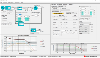
Below are Platinum simulation for filters as per schematic
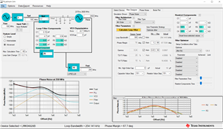
How can we minimize the frequency drift?

Should the internal loop filters or external filters of PLL2 to be varied to avoid the frequency drift?

Please suggest.

Since we are using only PLL2, What should be the PLL BW for optimized jitter?

What should be the Phase margin for optimized performance?

What should be the Open loop and closed loop Gain for  optimized performance?

Thanks.

  • Hi Team,

    Awaiting for your response.

    Thanks

  • Hello Lakshminarayana,

    To better help you, please attach your .tcs file and I can help you solve the problem. 

    To answer your general questions:

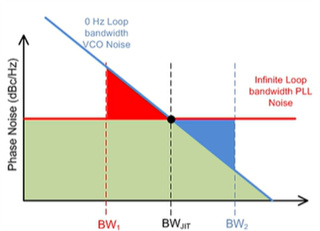
    In general, to minimize frequency drift, or decrease jitter at your output, you can increase your phase detector frequency, aim for a phase margin of 55 - 80 degrees, have your output type to be LVPECL if possible, and potentially a higher charge pump current could decrease jitter (however increase spurs). If none of these options are attainable for you (which seems to be your case), then you need to measure the PLL noise and VCO noise and determine where they intersect and add 25% to that value, that frequency offset will be where you want your LBW to be to minimize jitter (please refer to the picture below for a visual).

    For a more detailed explanation, PLL noise affects the overall noise of the device at lower frequencies (acts like a low-pass filter) and VCO noise affects the device at higher frequencies (acts like a high pass filter). Therefore, the intersection point between these two curves, + 25% of that value to account that the loop filter is not a brick wall filter, should be your loop BW and will optimize your jitter.

    Should the internal loop filters or external filters of PLL2 to be varied to avoid the frequency drift?

    Will answer this once I have your .tcs file and kniow your input and output frequencies, output type, etc. Even though I can deduce some of this from PLLatinum Sim screenshot, I need to corroborate those values for a better response. Hope this helps.

    Thanks,

    Andrea

  • Hi  ,

    I'll share you the tics file

    But anything to do with PLL2 Loop filters?

  • Hi 

    Please find the tcs file

    R0 (INIT)	0x000090
    R0	0x000004
    R2	0x000200
    R3	0x000306
    R4	0x0004D0
    R5	0x00055B
    R6	0x000600
    R12	0x000C51
    R13	0x000D04
    R256	0x01000A
    R257	0x010155
    R258	0x010255
    R259	0x010301
    R260	0x010422
    R261	0x010500
    R262	0x010670
    R263	0x010755
    R264	0x01086A
    R265	0x010955
    R266	0x010A55
    R267	0x010BB1
    R268	0x010C22
    R269	0x010D00
    R270	0x010E70
    R271	0x010F11
    R272	0x01106A
    R273	0x011155
    R274	0x011255
    R275	0x0113B1
    R276	0x011422
    R277	0x011500
    R278	0x011670
    R279	0x011733
    R280	0x01186A
    R281	0x011955
    R282	0x011A55
    R283	0x011BB1
    R284	0x011C22
    R285	0x011D00
    R286	0x011E71
    R287	0x011F03
    R288	0x012072
    R289	0x012155
    R290	0x012255
    R291	0x0123B1
    R292	0x012422
    R293	0x012500
    R294	0x012678
    R295	0x012755
    R296	0x012808
    R297	0x012955
    R298	0x012A55
    R299	0x012B00
    R300	0x012C02
    R301	0x012D00
    R302	0x012EF9
    R303	0x012F00
    R304	0x013016
    R305	0x013155
    R306	0x013255
    R307	0x013300
    R308	0x013402
    R309	0x013500
    R310	0x0136F1
    R311	0x013700
    R312	0x013805
    R313	0x013903
    R314	0x013A02
    R315	0x013B80
    R316	0x013C00
    R317	0x013D0E
    R318	0x013E03
    R319	0x013F05
    R320	0x014089
    R321	0x014100
    R322	0x014200
    R323	0x014321
    R324	0x0144FF
    R325	0x01457F
    R326	0x014618
    R327	0x01470A
    R328	0x014802
    R329	0x014942
    R330	0x014A02
    R331	0x014B16
    R332	0x014C00
    R333	0x014D00
    R334	0x014EC0
    R335	0x014F7F
    R336	0x015003
    R337	0x015102
    R338	0x015200
    R339	0x015300
    R340	0x01540A
    R341	0x015500
    R342	0x0156C5
    R343	0x015700
    R344	0x015896
    R345	0x015900
    R346	0x015A64
    R347	0x015BF4
    R348	0x015C20
    R349	0x015D00
    R350	0x015E00
    R351	0x015F0B
    R352	0x016000
    R353	0x016105
    R354	0x016245
    R355	0x016300
    R356	0x016400
    R357	0x01650C
    R369	0x0171AA
    R370	0x017202
    R380	0x017C15
    R381	0x017D33
    R358	0x016600
    R359	0x016700
    R360	0x016820
    R361	0x016959
    R362	0x016A20
    R363	0x016B00
    R364	0x016C00
    R365	0x016D00
    R366	0x016E13
    R371	0x017300
    R386	0x018200
    R387	0x018300
    R388	0x018400
    R389	0x018500
    R392	0x018800
    R393	0x018900
    R394	0x018A00
    R395	0x018B00
    R8189	0x1FFD00
    R8190	0x1FFE00
    R8191	0x1FFF53
    

  • Hello Lakshminarayana,

    You are correct, the loop filter could be the problem in your design. After looking at your .tcs file, the values for your Fpd and Fvco do not match the values from the screenshot of PLLatinum Sim; therefore, that's what resulted in the values on your screen (assuming you clicked on the "Calculate Loop Filter" button). After changing those values you had previously to the ones from your .tcs file, your loop filter should match the below setup to optimize jitter.

    Note, that the loop filter components are dependent on the PFD, charge pump, and VCO gain. Therefore, by having incorrect values, will lead to an incorrect loop filter design. In PLLatinum Sim, the Fvco also matter since that is also used in the code to properly obtain the VCO gain. If the values I suggested seem off, please make sure those three variables are correct in PLLatinum Sim and that way you can generate your own loop filter values.

    Another suggestion is increasing the PFD if my other suggestions don't work. Hope this helps.

    Good Luck,

    Andrea

  • Hi ,

    Why can't we change the internal loop filter?

    I was also asking on more details on this: 

    What should be the Open loop and closed loop Gain for  optimized performance?

    Since we are using only PLL2, What should be the PLL BW for optimized jitter?

    Hi

    Sorry,  in my previous Platinum Simulation Output frequency was set to 250MHz. It is supposed to be 256MHz

    Below are Platinum simulation for filters as per schematic
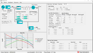
    Here It should be 256MHz

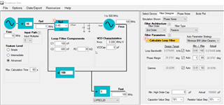
    This above simulation is based on our current board C1: 150pF; C2:4.7nF, R2: 560 Ohm: Internal loop filter are set to default values.

    With this jitter(fs) is 152.7 which seems to quite good. But the Loop BW is less of 124.411KHz and Phase Margin of 62.9 degree

    We will try out your suggestion of loop filter values and verify.

    Why in your simulation Loop filter BW is set to 400KHz?

  • Hello Lakshminarayana,

    Why can't we change the internal loop filter?

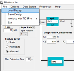
    You can change it! But only to the options given in TICS Pro by the drop-downs, as shown in the picture below.

    What should be the Open loop and closed loop Gain for  optimized performance?

    The open and closed loop gain have no effect on jitter; therefore, their values should not matter for this problem.

    Since we are using only PLL2, What should be the PLL BW for optimized jitter?

    The optimal PLL2 BW can be determine by obtaining the intersection point of the phase noise plot of the VCO and the phase noise plot of just the PLL. By obtaining those curves and their intersection point and incrementing that offset frequency by 25%, then that would be the optimal point to decrease jitter.

    Why in your simulation Loop filter BW is set to 400KHz?

    This was not done on purpose, you can ignore that value. That ended up being set that way because I was trying to obtain a higher phase margin value to decrease jitter.

    With this jitter(fs) is 152.7 which seems to quite good.

    I'm glad you found a solution for your system. If you keep facing any problems, please do let me know.

    Good Luck,

    Andrea

  • With this jitter(fs) is 152.7 which seems to quite good.

    I'm glad you found a solution for your system. If you keep facing any problems, please do let me know.

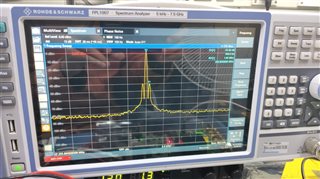
    The problem is not solved. We still have. Your suggestion values of filter improved a little. But still we have jitter as you can in the below image.

    Yellow trace: Max hold of RF Out

    Blue trace: Continuous trace.

    If jitter to be measured in spectrum analyzer, what setting of RBW and Span  do you recommend?

    With this jitter(fs) is 152.7 which seems to quite good.

    This I mentioned for PLatinum Simulation. Not on Board.

    The open and closed loop gain have no effect on jitter; therefore, their values should not matter for this problem.

    hen what effect Open and Closed loop gain will have? If not on jitter?

    The optimal PLL2 BW can be determine by obtaining the intersection point of the phase noise plot of the VCO and the phase noise plot of just the PLL. By obtaining those curves and their intersection point and incrementing that offset frequency by 25%, then that would be the optimal point to decrease jitter.

    Can you be more clearer with an example?

    Ideally what Loop BW for PLL2 do you recommend?

  • Hello Lakshminarayana,

    I am currently going through training until next week, so I won't be able to reply until then. Please do update me if anything changes.

    Best,

    Andrea

  • Hello Lakshminarayana,

    If jitter to be measured in spectrum analyzer, what setting of RBW and Span  do you recommend?

    We do not recommend using spectrum analyzers to measure jitter; we mainly use them to measure spurs. Instead, in our lab, we use a phase noise analyzer, do you have one available? If you'd like, I can obtain this values for you; however, I will be restricted to the values already chosen in our EVM. This way you can get an idea of the jitter I'm obtaining with the filter I am using (but not your exact values for jitter).

    what effect Open and Closed loop gain will have? If not on jitter?

    I am finalizing a correct answer for you on this, I will get back to you later.

    This I mentioned for PLatinum Simulation. Not on Board.

    What is your calculated phase noise on board? Ideally, please tell me this value after the changes I suggested below for your loop filter.

    Ideally what Loop BW for PLL2 do you recommend?

    I have re-run the simulation on PLLatinum Sim and have found a better solution than the one I posted previously, please look at values below:

    For future reference, to obtain the optimal LBW for your application:

    1) After creating your frequency plan and design that will optimize jitter, populate your Fpd, Kpd, and Fvco accordingly

    2) Make sure all check boxes are selected for "Auto" (as shown in the picture above)

    3) Under "Filter Optimizer," under the drop-down menu "Optimize," select "Jitter (fs)"

    4) Click on "Calculate Loop Filter" and wait about a minute or two to obtain optimal loop filter values for optimized loop bandwidth.

    By following the steps above, PLLatinum Sim will calculate the optimal loop bandwidth for you as well which you don't have to determine. For your case, the optimal loop bandwidth should be around 200 kHz. Hope this helps.

    Best,

    Andrea

  • Hi  Andrea Vallenilla

    Thanks for your response.

    I've below queries:

    I'm referring Xilinx Clock Eval Board: https://www.xilinx.com/content/dam/xilinx/support/documents/boards_and_kits/zcu216/ug1437-clk104.pdf

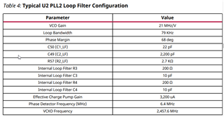
    A) As per his Loop filter configuration on page no: 14 (Table 14), Loop filter values are as below from Simulation,

    B) For the same above simulation, If I check the box of Jitter optimize options, I get different values of Loop filter values, 

    Of Above two which I should be considering A or B?

  • Hi,

    Another query,

    We have custom board with 160MHz VCXO (SiT3372): https://www.mouser.com/datasheet/2/371/SiT3372-datasheet-1153995.pdf

    https://www.digikey.in/en/products/detail/sitime/SIT3372AI-1B2-25NH160-000000/11764410

    We have below Loop filter:

    For PLL1:

    PLL1 PFD: 1MHz (Tried with PFD 5MHz too)

    For PLL2:

    We observe spur at 480Hz at LMK Output of level -50dBfc.

    When PLL1 is turned off, we do not see any spur.

  • Hello Lakshminarayana,

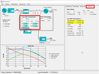
    I went ahead and redid the PLLatinum simulation from the (A) you described above (assuming you meant Table 4) and noticed some differences to your set-up. Based on the description on the document you attached, the loop filter values don't match the document because the GUI is looking at a different LBW and phase margin. Your screenshot says ~68 kHz when Table 4 says 79 kHz for LBW and your phase margin says ~55 degrees while the table specifies 68 degrees. When setting their specified loop filter value components, I obtained very similar LBW and phase degree values (my set-up included below):

    Of Above two which I should be considering A or B?

    If you ultimate goal is to optimize jitter, then I would suggest you pick B. If there are other considerations in your design (such as lock time), then maybe obtaining a different configuration could be best. This is design dependent. Hope this helps!

    Good Luck,

    Andrea

  • Hello Lakshminarayana,

    The loop filter does not cause spurs, but it can attenuate them. Instead, what could be causing the spur in your system is your VCXO or your reference signal. To test this, could you change the reference you are using? If you see the spur become smaller or disappear, then the source is the reference signal.

    Also, just to clarify I'm assuming you are trying to get rid of the spur? Thanks!

    Best,

    Andrea

  • Hi, Thanks for your reply. 

    We have checked both reference signal before LMK configuration, There was no spur. After LMK configuration, we are observing spur on VCXO, LMK clock output. 

    Is it because of VC of LMK?

  • Hi  Andrea Vallenilla

    I have re-run the simulation on PLLatinum Sim and have found a better solution than the one I posted previously, please look at values below:

    I've tried with the same loop filter suggested by you for PLL2 and For PLL1 Loop filter is as below, But still we have the spur at 350Hz with 100MHz VCXO 

    PLL1 Loop filter

    PLL2 Loop filter as suggested you.

    I have re-run the simulation on PLLatinum Sim and have found a better solution than the one I posted previously, please look at values below:

    Tested Part of 100MHz VCXO

    a) 515ACA100M000BAG (https://www.mouser.in/datasheet/2/472/Si515-2507350.pdf )

    b) V7223T (http://www.conwin.com/datasheets/vx/vx673.pdf )

    For the both parts below are observation

    • When LMK is not configured, we are observing clean 100MHz VCXO
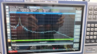
    • When LMK is configured, we are observing a spur of 350Hz (image below for reference of spectrum and Phase Noise)
      • At LMK Output
      •   \
    • Changing the loop filter didn't seem to change anything we have not noticed any changes in output behaviour.

    This doesn't seem to be reference clock spur.

    We have observed both the 10MHz Input and 100MHz VCXO, It doesn't have spur. But spur are observed after LMK Configuration

  • Hello Lakshminarayana,

    Just to clarify, you are still seeing the spur in PLL1 correct? That's what the data you included in your reply relates to? Also, the Kvco you have on the screenshot for PLL1 is wrong. One of the key parameters to properly calculate loop filter and LBW is the Kvco. To calculate the Kvco of your 2 VCXOs you included above, you need to take the typical tuning sensitivity and multiply it by your VCXO operating frequency. For instance, Kvco_conwin = typical tuning sensitivity * VCXO freq = 65 ppm/V * 100 MHz = 6.5 kHz/V or .0065 MHz/V. With this consideration this is the loop filter design you get when optimizing jitter. Note that I obtained the below two set-up a bit differently than before. In "Auto Parameter Strategy" I selected "Optimize Jitter" and I did not use the Performance Summary section:

    And this loop filter when balancing spurs (changed drop-down option to "Balance for Spurs":

    Feel free to try this for your other VCXO and see the results. I know you mentioned changing the loop filter values did not affect the spurs, but try the ones above and compute your own from the other VCXO and if it does not fix you problem, we can talk about other things that may be causing the spurs. Note that the PLL should not be causing the spur and the one good way to get rid of a spur is by attenuating it with a loop filter. Hope this helps.

    Good Luck,

    Andrea

  • Yes we are observing the spur at VCXO after LMK configured. i.e., PLL1 Configured. We were also getting spur with only PLL2 mode also.  

    We will try the above balanced spur loop filters and update you.

    Few questions:

    • What values of KPD Do you recommend for PLL1 For optimizing the jitter and spur

    • What values of KPD Do you recommend for PLL2 For optimizing the jitter and spur

    We also have another case, where in on tapping the board or FAN Noise is picked up by the VCXO and causing LMK Output noise floor to be increased around 2.5KHz. as mentioned in another case: https://e2e.ti.com/support/clock-timing-group/clock-and-timing/f/clock-timing-forum/1161865/lmk04828-lmk04828-noise-floor-issue-on-vibration/4378676#4378676 

    The VCXO used is: V7223T (http://www.conwin.com/datasheets/vx/vx673.pdf )

    Do you recommend any loop filters / any suggestions to overcome this?

  • Hi  Andrea Vallenilla

    For below cases, please recommend loop filter with tcs files if possible,

    Case1: 10MHz CLKIN0, VCXO-100MHz VCO:2560MHz , CLKOUT: 256MHz

    10MHz Part: https://www.digikey.in/en/products/detail/abracon-llc/AST3TQ53-T-10-000MHZ-5-C/5237064 

    Case2: 10MHz CLKIN0, VCXO-160MHz, VCO-2560MHz CLKOUT-256MHz

  • Hello  Lakshminarayana,

    I will get back to you by next week.

    Best,

    Andrea

  • Hello Lakshminarayana,

    Please find the files below for both cases to help you with your design. The default KPD given by TICS Pro should work well (use 0.45mA for PLL1s and 3.2mA for PLL2s). Note that the .sim files are loaded unto PLLatinum Sim directly.

    E2E_FrequencyDrift_case1.tcs

    https://e2e.ti.com/cfs-file/__key/communityserver-discussions-components-files/48/E2E_5F00_FrequencyDrift_5F00_case1PLL1.sim

    https://e2e.ti.com/cfs-file/__key/communityserver-discussions-components-files/48/E2E_5F00_FrequencyDrift_5F00_case1PLL2.sim

    E2E_FrequencyDrift_case2.tcs

    https://e2e.ti.com/cfs-file/__key/communityserver-discussions-components-files/48/E2E_5F00_FrequencyDrift_5F00_case2PLL1.sim

    https://e2e.ti.com/cfs-file/__key/communityserver-discussions-components-files/48/E2E_5F00_FrequencyDrift_5F00_case2PLL2.sim

    We also have another case, where in on tapping the board or FAN Noise is picked up by the VCXO and causing LMK Output noise floor to be increased around 2.5KHz. as mentioned in another case: https://e2e.ti.com/support/clock-timing-group/clock-and-timing/f/clock-timing-forum/1161865/lmk04828-lmk04828-noise-floor-issue-on-vibration/4378676#4378676 

    After reading the post, there is not much else we can help you with as the problem is coming from the accuracy of the VCXO since those are quite susceptible to vibrations. I would suggest to try the simulations I gave you above and test it again. Also, the same suggestions Ajeet/Timothy gave you, I would suggest you try those again as well since I have no further fixes for that problem. If this does not fix your problem, then I would suggest to talk to the VCXO's company's support team since it's their part causing the phase noise issues.

    Do you recommend any loop filters / any suggestions to overcome this?

    Again, I would suggest looking at other oscillators (potentially one from TI) if this keeps occurring. General idea is to lower the BW of PLL1, but the BW is already pretty low and lowering it can do so much.

    If you have any other questions, please first test all of this files, and then please outline which steps are complete and which you are stuck on. I can provide further explanation on that topic if needed (just as you did on your last reply, that was significantly more helpful).

  • Hi  Andrea Vallenilla,

    If you can provide me a snapshot Platinum sim tool loop filter calculation for the above cases that would be helpful.

    For Kpd-0.15, also can you please suggest me loop filter values of vcxo-100MHz, 160Mhz

    Lowering the Kpd would affect much?

  • Hello Lakshminarayana,

    Did the .sim files not work for you? You can load them into PLLatinum Sim as below, that way you are testing exactly what I gave you.

    Also, I forgot to add to that my answer used a VCXO control voltage tuning slope of 60 ppm/V (which translates to Kvco = 0.006 MHz/V). Make sure to choose that when you program the VCXO. I got the value from a table below, located in the VCXO data sheet you provided.

    For Kpd-0.15, also can you please suggest me loop filter values of vcxo-100MHz, 160Mhz

    You can calculate these values for the loop filter yourself. All you have to do is in the .sim file that I sent, just select the Kpd of 0.15 mA from the drop down menu and click on "Calculate Loop Filter," as shown in the image below. That should give you the new loop filter values.

    Lowering the Kpd would affect much?

    Lowering the charge pump current (Kpd) would significantly lower the loop bandwidth and can lower phase noise/jitter. However, this fix only lowers the reference's and PLL phase noise profile, so if the VCO phase noise profile is worse than either of those two, then the effect of decreasing the charge pump is insignificant. Hope this helps!

    Good luck,

    Andrea

  • I would suggest looking at other oscillators (potentially one from TI)

    Does TI Supports VCXO?

  • Hi  

    I've tried this spurfree loop filter values suggested by you, We still have the issue of Vibration noise

    And this loop filter when balancing spurs (changed drop-down option to "Balance for Spurs":

  • Hi Lakshminarayana,

    TI doesn't support VCXO. 

    Regarding the vibration noise with the VCXO, as we suggested, please check with the vendor and they can give some details on it.

    Thanks!

    Regards,
    Ajeet Pal