This thread has been locked.

If you have a related question, please click the "Ask a related question" button in the top right corner. The newly created question will be automatically linked to this question.

LMK04828BEVM: Clk_In and OSC difference

Part Number: LMK04828BEVM
Other Parts Discussed in Thread: AFE7906, LMK04828

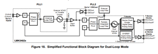
I have AFE7906 ADC , need to give device clock and Sysref for ADC and FPGA  from LMK04828 ,can we connect both OSCin and clkin pins

  • Hello Rajashekar,

    You can use both OSCin and CLKin pins but not at the same time, either the CLKin pin signal will act as reference or the OSCin reference will. If this wasn't your question, please further elaborate so I can better support you.

    Do note that the OSCin is the input to the second PLL; therefore, the reference signal inputted to OSCin would completely skip the first PLL and omit any jitter cleaning done by it. FYI, the first PLL is used to clean the reference inputted to our device and the second PLL is used to generate higher output frequencies.

    Also note, that if you are inputting a signal to the OSCin pin and using this pin as a clock input, then the CLKin input signal that goes through the first PLL won't go through the second PLL. Please look at the picture below from p. 50 in the data sheet to better understand how the signal travels through our device.

    Thanks,

    Andrea