Other Parts Discussed in Thread: TIDA-01021, LMK61E2,
Hi, all:
I have a question about digital lock of PLL1 in the LMK04828B.
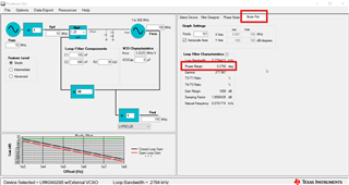
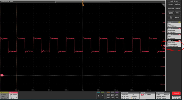
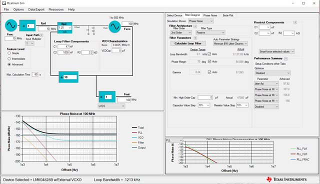
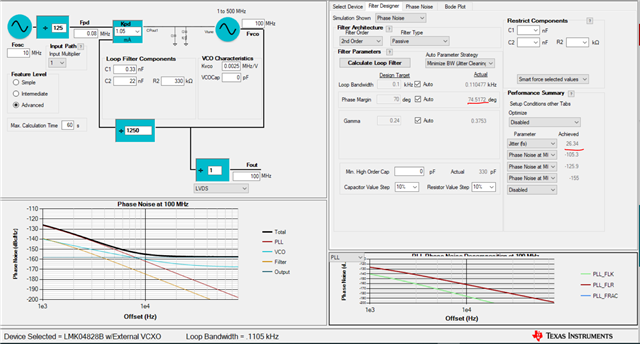
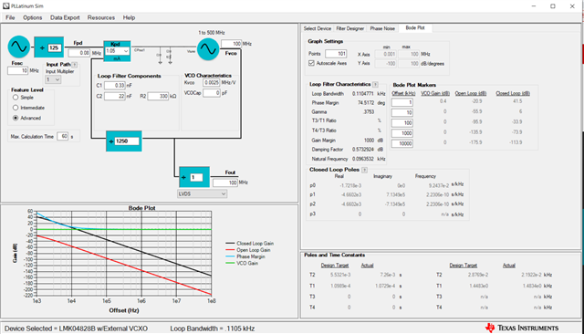
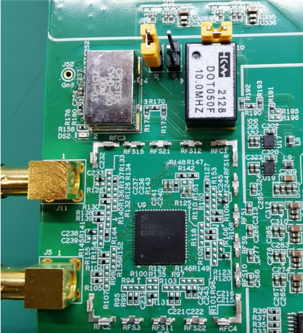
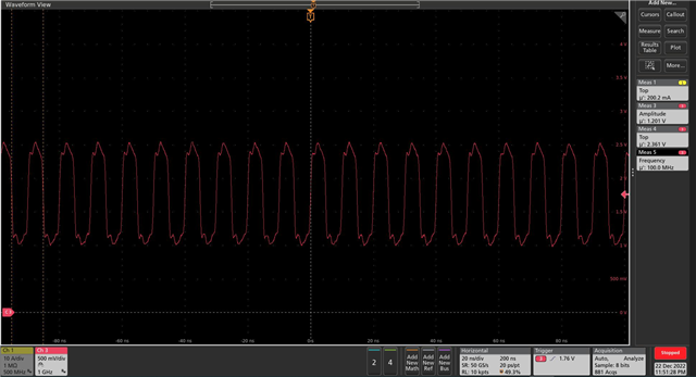
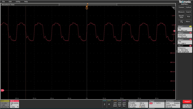
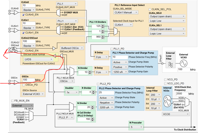
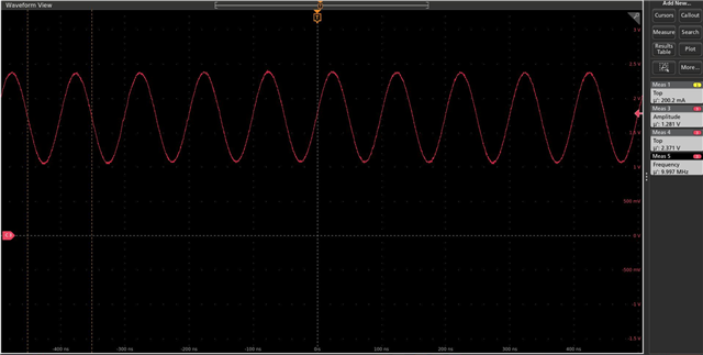
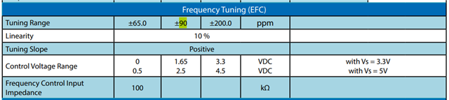
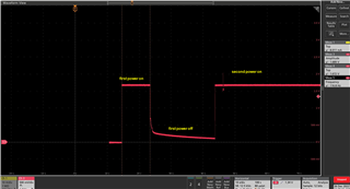
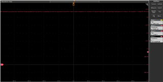
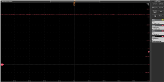
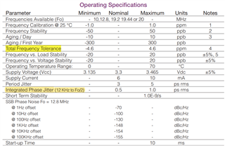
As below figure.1 shown, I supply a 10MHz from TCXO to CLKin1, Fpd is set to 10MHz, and external VCXO is 100MHz which is the same as VCXO on the TIDA-01021. The LED for PLL1 DLD can't be lighten, but when this LED is switched to PLL2 DLD, it will be lightened. The figure.2 is parameter of 10MHz TCXO, and figure.3 is the 100MHz VCXO. I also test 100MHz from VCXO to OSCin of LMK04828B as below figure.4 shown, it is OK. The capacity and resistor in the loop filter are the same design with TIDA-01021 too(C1=0.1uF, C2=0.68uF and R2=39kohm)
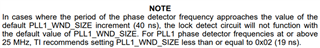
I also notice the "10.2 Digital Lock Detect Frequency Accuracy", so try to change PLL1_DLD_CNT from 8192 to 5000 and keep the PLL1_WND_SIZE as 43ns. but it doesn't work.
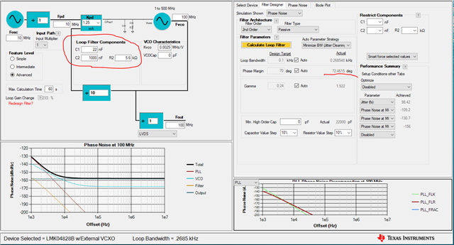
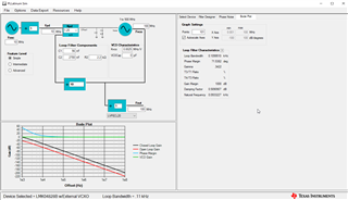
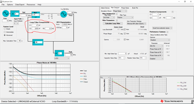
At last, I use PLLatinum Sim to simulate PLL1 based on above loop filter, it seems that the phase noise curve is not good.
Could you please help me check what is wrong in my setup? or point out correct way to make PLL1 lock?
Thanks in advance!
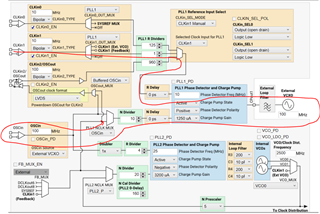
figure.1
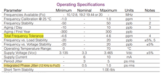
Figure.2
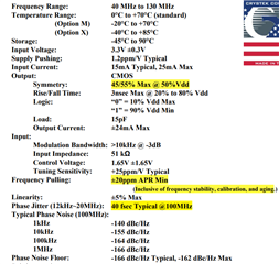
Figure.3
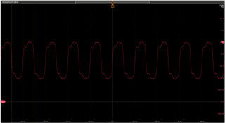
Figure.4
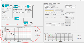
Figure.5
Best regards!
Jason