This thread has been locked.

If you have a related question, please click the "Ask a related question" button in the top right corner. The newly created question will be automatically linked to this question.

LMK03318: Current consumption

Part Number: LMK03318
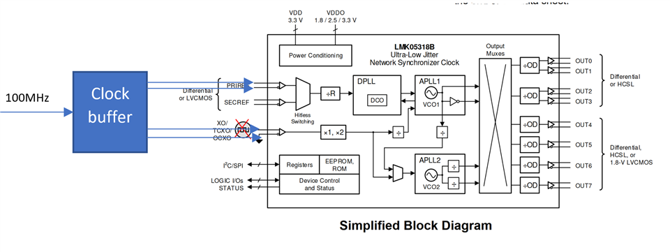
Other Parts Discussed in Thread: CDCI6214, , LMK05318B

Hi,

I am going to use a LDO to support clean power to the clock chips on my board, so I need to evaluate the current of LMK03318. There are three types of current consumption spec in datasheet page9. I should add the “core current consumption, per block” and “Current consumption, per supply pin” together to get total supply current, am I right? The “Output current consumption, per block” spec is include in the “Current consumption, per supply pin”, right? I am going to generate 7 channel LVPECL clocks and 1 channel LVCOM-1.8V clock.

Then I get very large current value close to 1A. why the current consumption is so large? I also need to use CDCI6214 in my design, that power spec in the datasheet is only 150mW. For 1.8V power supply, the current is only 80mA that is much more lower than LMK03318. What mistake do I have.

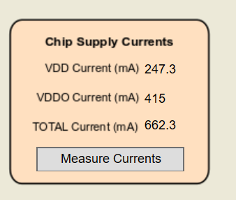
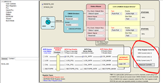
In TICS Pro software, there is one spec call “Chip Supply Current” in “Status” table. May I use this one to get correct current base on the design? Why they are always 0mA? How to make it work?

 Regards,
Shu

  • Shu,

    You can load a configuration into TICS Pro and get the output current if an EVM is connected, per this thread: https://e2e.ti.com/support/clock-timing-group/clock-and-timing/f/clock-timing-forum/1171337/lmk03318-power-consumption-calculation/4412228?tisearch=e2e-sitesearch&keymatch=LMK03318%25252520current#4412228

    This functionality is not supported if not connected to an actual device, as it is a read of the device's ADC measurement.

    In the example from the above thread, when the device has all outputs set to AC-CML (the configuration file can be uploaded in the Raw Registers page), the measured current is 63-64mA. Note that the value in the table in the datasheet is larger - it fully depends on the settings for the inputs, PLL, and outputs. If, for example, if OUT4 through OUT7 are unused, then their currents would not be present in the overall current.

    The easiest way to determine current consumption is to create the configuration in TICS Pro, load it onto an LMK03318EVM, provide the supply voltages, and read the ADC currents from the device.

    Thanks,

    Kadeem

  • Hi Kadeem,

    Is it possible to evaluate the current using the datasheet? I ordered one EVM board, but it won’t ship to us quickly.

    In my question, I use the datasheet to simulate a 1A current consumption when use 7 channel LEVPECL output and 1 channel 1.8V LVCOMS output. In your link, the customer current consumption from TICS Pro is only 64mA. Our application may be different, but the current difference should’ be so large. How could I get a rational current consumption by datasheet?

    I saw you can help me to evaluate the power if I can provide the design file. So I upload the design file and register file, could you please help me to evaluate it? I wish to compare the results from datasheet and software.

    Regards,
    Shu

    0576.HexRegisterValues.txt
    R0	0x0010
    R1	0x010B
    R2	0x0232
    R3	0x0300
    R4	0x0400
    R5	0x0500
    R6	0x0600
    R7	0x0700
    R8	0x0800
    R9	0x0900
    R10	0x0A00
    R11	0x0B00
    R12	0x0C9F
    R13	0x0D00
    R14	0x0E00
    R15	0x0F00
    R16	0x1000
    R17	0x1100
    R18	0x1200
    R19	0x1300
    R20	0x14FF
    R21	0x15FF
    R22	0x16FF
    R23	0x1702
    R24	0x1800
    R25	0x19F5
    R26	0x1A00
    R27	0x1B58
    R28	0x1C58
    R29	0x1D00
    R30	0x1E00
    R31	0x1F30
    R32	0x2030
    R33	0x2117
    R34	0x2230
    R35	0x237C
    R36	0x2417
    R37	0x2518
    R38	0x261D
    R39	0x2718
    R40	0x281D
    R41	0x2918
    R42	0x2A1D
    R43	0x2B18
    R44	0x2C1D
    R45	0x2D3A
    R46	0x2E00
    R47	0x2F00
    R49	0x3100
    R50	0x3252
    R51	0x3303
    R52	0x3400
    R53	0x3500
    R54	0x3601
    R55	0x3700
    R56	0x3806
    R57	0x3908
    R58	0x3A00
    R59	0x3B3C
    R60	0x3C00
    R61	0x3D00
    R62	0x3E00
    R63	0x3F00
    R64	0x4000
    R65	0x4101
    R66	0x420C
    R67	0x4304
    R68	0x4401
    R69	0x4504
    R70	0x4607
    R71	0x4707
    R72	0x4808
    R73	0x4900
    R74	0x4A78
    R75	0x4B00
    R76	0x4C00
    R77	0x4D00
    R78	0x4E00
    R79	0x4F00
    R80	0x5001
    R81	0x510C
    R82	0x5210
    R83	0x5301
    R84	0x5404
    R85	0x5507
    R86	0x5608
    R87	0x5700
    R88	0x5800
    R89	0x59DE
    R90	0x5A01
    R91	0x5B18
    R92	0x5C01
    R93	0x5D4B
    R94	0x5E01
    R95	0x5F86
    R96	0x6001
    R97	0x61BE
    R98	0x6201
    R99	0x63FE
    R100	0x6402
    R101	0x6547
    R102	0x6602
    R103	0x679E
    R104	0x6800
    R105	0x6900
    R106	0x6A05
    R107	0x6B0F
    R108	0x6C0F
    R109	0x6D0F
    R110	0x6E0F
    R115	0x7308
    R116	0x7419
    R117	0x7500
    R118	0x7607
    R119	0x7705
    R120	0x7800
    R121	0x790F
    R122	0x7A0F
    R123	0x7B0F
    R124	0x7C0F
    R129	0x8108
    R130	0x8219
    R131	0x8300
    R132	0x8407
    R133	0x8505
    R134	0x8600
    R135	0x8700
    R136	0x8800
    R137	0x8910
    R138	0x8A00
    R139	0x8B00
    R140	0x8C00
    R141	0x8D00
    R142	0x8E00
    R143	0x8F00
    R144	0x9000
    R145	0x9100
    R169	0xA940
    R172	0xAC24
    R173	0xAD00
    
    my design.tcs

  • Shu,

    You are correct - based on the datasheet values, I too would expect far larger current. I will evaluate this on a board and have a response for you by Monday.

    Thanks,

    Kadeem

  • Shu,

    When I load the configuration into the device, I get the following:

    I discussed this with my manager as well based on the old E2E thread, and he confirmed that a current in the range that I have displayed here is expected.

    Thanks,

    Kadeem

  • Thank you very much. I will evaluate my power plan use above current values.

  • Shu,

    My pleasure. Please do not hesitate to reach out if you have any further questions.

    Thanks,

    Kadeem

  • Hi Kadeem,

    i found the PDN pin is internal pullup to VDDO_01 in the datasheet. This pin could be connected to a external pullup resistor too. but the LMMK03318EVM board connect this pin to VDD_R which is the core votlage through a 13K resistor R127. Should i connect this pin to VDDO_01 or core voltage if my VDDO_01 is 1.8V. why the EVM connect it to core voltage?

    Regards,
    Shu

  • Shu,

    The pin is able to be pulled up to either 3.3 V or 1.8 V. The PDN pin is rated for maximum 3.6 V, and recognizes a logical low at 0.6 V (with logical high at 1.2 V)  You can connect this to either VDDO_01 or VDD_R (the core voltage) in your design.

    The EVM designer chose to use the VDDO_01 voltage exclusively for the supply for OUT0 and OUT1, with all of the buttons connected to the core voltage.

    Thanks,

    Kadeem

  • Thank you Kadeem,

    one more thing, i am going to use the auto switch function. the primary input is an LVPECL clock, the secondary input is a LVCMOS clock from an active oscillator. Both frequency is 100MHz. Do I need to transfer the LVCMOS clock to LVPECL to secondary input? I know I can make the primary input to differential and secondary to single-end in the software. But use the auto switch function to change reference input, would it be better to use same type input?

    The oscillator is 1.8V power supply. The VIH min is only 1.4V, looks like I can connect it directly to second input. but how about I connect to negative pin of second input to a 0.9V reference voltage that is a regular way to drive single-end single to differential input, the swing could be 0.9V. I fell it is better than the way to connect 1.8V oscillator to second input. But I don’t find such modes in the datasheet, does the LMK03318 support this way? which way is better?

    I have one more question about LMK05318B. I won’t do it, but I wish to make clear. The LMK05318B has to use a XO or other reference to the XO pin. Then another clock go to reference input to synchronize. How about I use one source and separate it to two clocks using a buffer, then connect them to the reference input and XO input of LMK05318B, will that work?

    Regards,
    Shu

  • Shu,

    I have the following responses:

    • the primary input is an LVPECL clock, the secondary input is a LVCMOS clock from an active oscillator. Both frequency is 100MHz. Do I need to transfer the LVCMOS clock to LVPECL to secondary input? But use the auto switch function to change reference input, would it be better to use same type input?
      • The two inputs are independent, and can be different clock formats. The important details for using the auto switching functionality are below
    • The oscillator is 1.8V power supply. The VIH min is only 1.4V, looks like I can connect it directly to second input. but how about I connect to negative pin of second input to a 0.9V reference voltage that is a regular way to drive single-end single to differential input, the swing could be 0.9V. I fell it is better than the way to connect 1.8V oscillator to second input. But I don’t find such modes in the datasheet, does the LMK03318 support this way? which way is better?
      •  If using a single-ended input, pull the XO_N pin to GND, per the datasheet. No other configuration of the SECREF_N pin for single-ended inputs is supported. The input buffer of this pin supports single-ended inputs
    • The LMK05318B has to use a XO or other reference to the XO pin. Then another clock go to reference input to synchronize. How about I use one source and separate it to two clocks using a buffer, then connect them to the reference input and XO input of LMK05318B, will that work?

    Thanks,

    Kadeem

  • Thank you very much Kadeem,

    So i can use the 1.8VCMOS oscillator, right?

    About the LMK05318B question. I can’t open that two link. But my question wish to confirm may I use below way to use one clock source. Just for my curiosity.

    Regards,
    Shu

  • Shu,

    Using an LVCMOS clock instead of an XO will work here.

    Thanks,

    Kadeem