This thread has been locked.

If you have a related question, please click the "Ask a related question" button in the top right corner. The newly created question will be automatically linked to this question.

LMK04828: Why SYNC output of LMK04828B to LMX2594 are not stable during every power up?

Part Number: LMK04828
Other Parts Discussed in Thread: LMX2594, LMK61E2

Hi,

In my design, I use one LMX04828B to provide reference clock and Sync signal to four LMK2594.  Sync signal are used for aligning  SYSREF clock(4.8828125MHz) form  RFoutB of four LMK2594.

But I found that sometimes the four SYSREF clocks could be aligned completely after power on, and sometimes not.  Could you please help me check this issue? May be some mistake in the procedure? 

After power on, the sequence of clock configuration is:  LMK04828 1st configuration(basic configuration) -> LMK2594 configuration -> LMK04828 2st configuration(generate Sync to LMX2594) 

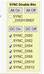
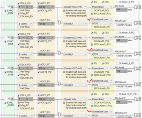
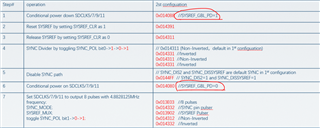
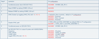
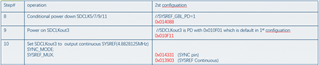
LMK04828 1st configuration, and SDCLK5/7/9/11 are ready for 4 SYNC signals;  DCLK2 and SDCLK3 are provided to FPGA

LMK61E2_100M_SinglePLL_PD 25M_LMX2594_4 SYNC.tcs

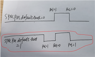
LMK04828 2st configuration: total 17 register operation marked with red is to make SDCLK5/7/9/11 output 8 continuous pulse with 4.8828125Mhz as SYNC signal for 4 LMX2594

The INPIN_LVL of LMX2594 is set as Vin because default value with Vin/4 don't take effect

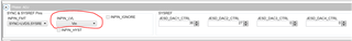
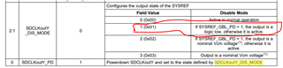
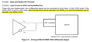
output format of SDCLK5/7/9/11 is LVDS, so SYNC format of LMX2594 is set according to below figure. The C215 and C216 have been replaced with 0 ohm resistors

Thanks in advance!!!

Best regards!

Jason

  • Hello Jason,

    I am currently running a test in the lab and won't be able to replicate this in lab until tomorrow; therefore, please expect a response back from me by latest Wednesday. Thanks!

    Best,

    Andrea

  • Hi, Andrea:

    Get it! I will wait for your response!

    Please help me check the configuration procedure, especially LMK04828 2st configuration.

    Many thanks to you:)

    Best regards!

    Jason

  • Hello Jason,

    Unfortunately, the board I have with me is not working and I cannot replicate your problem. I just requested to get  anew board, but I wont be able to get it until end of next week, that's when I'll be able to replicate your setup and tell you in more detail what may be going on (if still needed).

    In the mean time I think I may know what's going on. I was looking at your 2nd configuration and I'm not sure about the order of the steps you implemented plus certain register choices that may be incorrect. Therefore, I have listed the steps below explain a general step by step guide of how to achieve SYSREF phase alignment via the SYSREF pulser funcitonality. Note that I'm assuming the output registers (or the "Clock Outputs" page in TICS PRO) are not changed and they remain constant to the .tcs file you attached:

    1) SYNC_POL = 0, SYNC_MODE = 1 (SYNC Pin), SYSREF_MUX = 0 (Normal SYNC). 

    2) SYSREF_GBL_PD = 1, SYSREF_PD = 0, SYSREF_DDLY_PD = 0, SYSREF_PLSR_PD = 0, SYSREF_PULSE_CNT = 1 (2 pulses).

    3) Set local SDCLKoutX_DDLY register to correct cycles to achieve alignment across SYSREF clock cycles (if you don't know what to set each SYSREF clock to, look at note below *)

    4) SYNC_DISSYSREF = 0. Apart from this, I would try to see if your problem is fixed by setting SYNC_DIS6, SYNC_DIS8, SYNC_DIS10, and SYNC_DIS12 to 0, as well.

    5) Toggle SYNC by SYNC_POL = 1, right after SYNC_POL = 0.

    6) Disable SYNC from resetting dividers by SYNC_DISSYSREF = 1. If testing idea from #4, make sure to also set SYNC_DIS6, SYNC_DIS8, SYNC_DIS10, and SYNC_DIS12 to 1.

    7) SYSREF_CLR = 0 (needs to be set only for 15 distribution cycles)

    8) SYNC_MODE = 2 (SYNC Pin Pulser), SYSREF_MUX = 2 (SYSREF Pulser).

    9) Toggling SYNC will result in 2 SYNC pulses

    * To determine the cycles between the different SYSREF outputs, run through steps 1-9 without completing step 3 and notice the delays between the SYSREF clocks and apply that number to step 3 when going through these steps again to finally align the SYSREF edges.

    Let me know if this solved your problem!

    Best,

    Andrea

  • Hi, Andrea:

    I need it, and please  replicate my setup on your new board. I very appreciate it.

    About general step, I think it come from section 9.3.2.1.1  in the datasheet. Please see my words marked red:

    1) SYNC_POL = 0, SYNC_MODE = 1 (SYNC Pin), SYSREF_MUX = 0 (Normal SYNC). 

    2) SYSREF_GBL_PD = 1, SYSREF_PD = 0, SYSREF_DDLY_PD = 0, SYSREF_PLSR_PD = 0, SYSREF_PULSE_CNT = 1 (2 pulses).

    3) Set local SDCLKoutX_DDLY register to correct cycles to achieve alignment across SYSREF clock cycles (if you don't know what to set each SYSREF clock to, look at note below *)

    4) SYNC_DISSYSREF = 0. Apart from this, I would try to see if your problem is fixed by setting SYNC_DIS6, SYNC_DIS8, SYNC_DIS10, and SYNC_DIS12 to 0, as well.

    [Jason]: I won't use  DCLK6/8/10/12, so they are power down in 1st configuration.  I think it's no necessary to set SYNC_DIS6, SYNC_DIS8, SYNC_DIS10, and SYNC_DIS12 to 0.  Just  SDCLK5/7/9/11 are used for 4 SYNC signals and DCLK2/SDCLK3 are used for FPGA. In the 1st configuration SYNC_DIS2=0 and SYNC_DISSYSREF=0. After finishing SYNC divider, SYNC_DIS2 and SYNC_DISSYSREF will be set 1

    5) Toggle SYNC by SYNC_POL = 1, right after SYNC_POL = 0.

    [Jason]: Is a rise edge or fall rise needed to trigger resetting divider through toggling SYNC by SYNC_POL ?

    As below figure shown, the default  level of  SYNC pin in my board is high, so I set SYNC_POL =1 then 0 then 1 to get the similar effect with SYNC_POL =1 then 0 required by you

    6) Disable SYNC from resetting dividers by SYNC_DISSYSREF = 1. If testing idea from #4, make sure to also set SYNC_DIS6, SYNC_DIS8, SYNC_DIS10, and SYNC_DIS12 to 1.

    7) SYSREF_CLR = 0 (needs to be set only for 15 distribution cycles)

    [Jason]: Since this step to set SYSREF_CLR = 0, when did SYSREF_CLR set to 1 in the previous set?

    8) SYNC_MODE = 2 (SYNC Pin Pulser), SYSREF_MUX = 2 (SYSREF Pulser).

    9) Toggling SYNC will result in 2 SYNC pulses

    The other questions:

    1. What is the unit of SYSREF_DDLY?  also  is the number of VCO cycle? 

    2. How to understand half step function? For example, if SDCLKoutY_DDLY = 0x1 (delay 2 cycles) and SDCLKoutY_HS =1, then total delay cycle = ?

    Datasheet don't detailedly describe half step function 

    Thanks in advance!

    Best regards

    Jason

  • Hello Jason,

    I'll get back to you tomorrow.

    Best,

    Andrea

  • Hi, Andrea:

    OK.

    BTW, besides these questions in my last post, I add one question:

    SDCLKoutY_DIS_MODE in my 1st configuation is set to 0x1. In your step.2,  you set SYSREF_GBL_PD to 1.   But SYSREF_GBL_PD  is never set to 0 in your next steps that means SDCLK5/7/9/11 will always be logic low, right? Then,  how do SDCLK5/7/9/11 output 2 SYNC pulses through toggling SYNC in your step.9 ? 


    In my 2st configuration, SYSREF_GBL_PD is set to 0 before outputting 2 SYNC pulses through toggling SYNC as below figure shown.

    Is my understanding about SYSREF_GBL_PD is not same with you?

    Thanks in advance!!!

    best regards!

    Jason

  • Hello Jason,

    I was not able to get to your questions today and will be out of office later, so I have talked to my coworker to answer for me. He should get back to you by next week.

    Best,

    Andrea

  • Hi Jason,

    I just wanted to follow up on the above issue. Is that still open?

    If yes, I would prefer, if you can provide some simple block diagram of the clock connection. Why, I could not figure it out, what are the reference clocks (100M) from LMK04828 to LMX2594 are driving and are those aligned to each other (i.e. LMK outputs are synchronized) after your first configuration.

    Theoretically, in the beginning the LMK04828 outputs (DCLKs and SDCLKs) should be aligned (deterministic phase) and when the clocks are fed to LMX2594 then input SYNCs to LMX should maintain the setup and hold timing requirement to synchronized LMX outputs. i.e. SYNC input (rising edge) to LMX should be at least before 2.5ns from OSCin rising edge and should be high at least for 2ns.   

    Thanks!

    Regards,
    Ajeet Pal