This thread has been locked.

If you have a related question, please click the "Ask a related question" button in the top right corner. The newly created question will be automatically linked to this question.

LMK04832: LMK04832 Distribution mode

Part Number: LMK04832
Other Parts Discussed in Thread: LMX2820, LMX2594, LMK04828

Dear sir or madam,

I am trying to make the synchronous multiple clocks for multi-beam antenna.

I tested some modes of LMK04832 to use the EV board, but i couldn't find out the good setup for LMK04832.

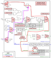
For your understanding, please refer to our topology of clock system.


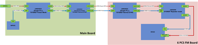
There are two types of board in our unit.

One is a main board which makes a SYSREF Clock and distributes the 10 MHz Reference clock and SYSREF to FM Boards.

The other are 6 FM Boards which are included DAC & ADC with RFSOC, and there are LMK04832 and LMX2694 in every FM boards.

In my test, there are several questions of setup for LMK04832.

Please refer to the following question and please give your advice.

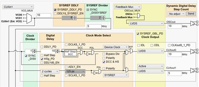
1. In Main Board, About Clock Distribution mode

 - input : SYSREF - From Signal Generator RF out to CLKin0, 10 MHz - From Signal Generator 10MHz out to CLKin1

 - PLL Raw register data

LMK04832_distribution mode.txt
R0 (INIT)	0x000090
R0	0x000010
R2	0x000200
R3	0x000306
R4	0x000463
R5	0x0005D1
R6	0x000670
R12	0x000C51
R13	0x000D04
R256	0x010001
R257	0x01010A
R258	0x010200
R259	0x010340
R260	0x010420
R261	0x010500
R262	0x010601
R263	0x010711
R264	0x010801
R265	0x01090A
R266	0x010A80
R267	0x010B50
R268	0x010C30
R269	0x010D00
R270	0x010E01
R271	0x010F11
R272	0x011001
R273	0x01110A
R274	0x011200
R275	0x011340
R276	0x011420
R277	0x011500
R278	0x011601
R279	0x011711
R280	0x011801
R281	0x01190A
R282	0x011A00
R283	0x011B40
R284	0x011C20
R285	0x011D00
R286	0x011E01
R287	0x011F11
R288	0x012001
R289	0x01210A
R290	0x012200
R291	0x012340
R292	0x012420
R293	0x012500
R294	0x012601
R295	0x012711
R296	0x012801
R297	0x01290A
R298	0x012A00
R299	0x012B40
R300	0x012C20
R301	0x012D00
R302	0x012E01
R303	0x012F11
R304	0x013001
R305	0x01310A
R306	0x013200
R307	0x013340
R308	0x013420
R309	0x013500
R310	0x013601
R311	0x013711
R312	0x013851
R313	0x013900
R314	0x013A00
R315	0x013B02
R316	0x013C00
R317	0x013D08
R318	0x013E03
R319	0x013F07
R320	0x0140FF
R321	0x014100
R322	0x014200
R323	0x014310
R324	0x01447F
R325	0x014520
R326	0x014618
R327	0x014700
R328	0x014802
R329	0x014902
R330	0x014A03
R331	0x014B06
R332	0x014C00
R333	0x014D00
R334	0x014EC0
R335	0x014F7F
R336	0x015001
R337	0x015102
R338	0x015200
R339	0x015300
R340	0x015478
R341	0x015500
R342	0x015601
R343	0x015700
R344	0x015896
R345	0x015900
R346	0x015A78
R347	0x015BD4
R348	0x015C20
R349	0x015D00
R350	0x015E1E
R351	0x015F0B
R352	0x016000
R353	0x016101
R354	0x01624C
R355	0x016300
R356	0x016400
R357	0x01650C
R361	0x016958
R362	0x016A20
R363	0x016B00
R364	0x016C00
R365	0x016D00
R366	0x016E13
R371	0x017370
R375	0x017700
R386	0x018200
R387	0x018300
R358	0x016604
R359	0x016700
R360	0x01680C
R1365	0x055500

(Q1) There are no output signals in every CLKOUT even ports - Device Clock 10 MHz.

        Would you find out why is not operated in this mode?

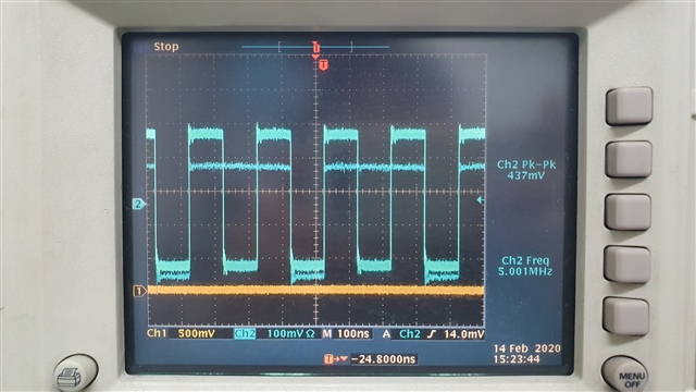
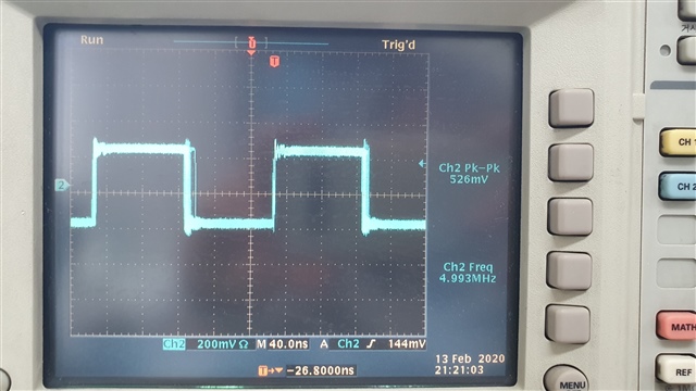
(Q2) In spite of getting the outputs in CLKOUT odd ports, but it look like having a jitter in SYSREF such as the picture.

        How do i reduce this jitter in clock output?

3. In FM board, About Repeater Mode

 - input : SYSREF  to SYSREFREQ, 250 MHz to OSCIN

 - PLL Raw register data

LMX2694 5GHz Repeater Mode.txt
R114	0x720000
R113	0x710000
R112	0x700000
R111	0x6F0000
R110	0x6E0000
R109	0x6D0000
R108	0x6C00F1
R107	0x6B0000
R106	0x6A0007
R105	0x694440
R104	0x680000
R103	0x670000
R102	0x660000
R101	0x650000
R100	0x640000
R99	0x630000
R98	0x620000
R97	0x610000
R96	0x600000
R95	0x5F0000
R94	0x5E0000
R93	0x5D0000
R92	0x5C0000
R91	0x5B0000
R90	0x5A0000
R89	0x590000
R88	0x580000
R87	0x570000
R86	0x560000
R85	0x550000
R84	0x540000
R83	0x530000
R82	0x520000
R81	0x510000
R80	0x500000
R79	0x4F0000
R78	0x4E0064
R77	0x4D0000
R76	0x4C000C
R75	0x4B0800
R74	0x4A0000
R73	0x49003F
R72	0x48003C
R71	0x47004C
R70	0x46C350
R69	0x450000
R68	0x4403E8
R67	0x430000
R66	0x4201F4
R65	0x410000
R64	0x401388
R63	0x3F0000
R62	0x3E0322
R61	0x3D00A8
R60	0x3C09C4
R59	0x3B0001
R58	0x3A0001
R57	0x390020
R56	0x380000
R55	0x370000
R54	0x360000
R53	0x350000
R52	0x340420
R51	0x330080
R50	0x320000
R49	0x314180
R48	0x300300
R47	0x2F0300
R46	0x2E07FE
R45	0x2DC0DF
R44	0x2C1F23
R43	0x2B0000
R42	0x2A0000
R41	0x290000
R40	0x280000
R39	0x27DA80
R38	0x26FD51
R37	0x258104
R36	0x240028
R35	0x230004
R34	0x220000
R33	0x211E21
R32	0x200393
R31	0x1F43EC
R30	0x1E318C
R29	0x1D318C
R28	0x1C0488
R27	0x1B0002
R26	0x1A0DB0
R25	0x190624
R24	0x18071A
R23	0x17007C
R22	0x160001
R21	0x150401
R20	0x14F048
R19	0x1327B7
R18	0x120064
R17	0x11012C
R16	0x100080
R15	0x0F064F
R14	0x0E1E70
R13	0x0D4000
R12	0x0C5004
R11	0x0B0018
R10	0x0A10D8
R9	0x090604
R8	0x082000
R7	0x0700B2
R6	0x067802
R5	0x0503E8
R4	0x040E43
R3	0x030642
R2	0x020500
R1	0x01080B
R0	0x00609C

(Q3) Are there nothing setup of SYSREF, if SYSREF_EN and SYSREF_REPEAT are on?

        Is it  just repeated according to the following to SYSREFREQ input signal, am i understanding right?

4. About Synchronous all of Clock

(Q4) To achieve the Synchronous between all of FM boards, is there any other recommendation for me? please give your advice.

Thank you,

Best Regards,

  • Hi Han,

    Whenever clock divider value is  =1, DCC & HS bit should be =1. 

    The jitter could be due to input 10MHz clock being a sine wave signal, try use square wave signal, for example use a function generator instead of RF generator to generate the input clock.

    Right, after setting up LMX2694 in sysref repeater mode, signal output from RFoutB will be equal to the input signal at sysrefreq pin.

    Synchronization is a complicated topic, it is hard to tell everything here. Suggest visit the product pages (LMX2694, LMX2594, LMX2820, LMK04832, LMK04828) for colleterial on sysref and synchronization.  

    BTW, your system phase noise is not going to be ideal. The 10MHz clock going to the LMK04832 in FCM board has accumulated jitter in the main board. Using this dirty10MHz clock to generate a 250MHz clock is also not ideal. Phase noise from LMK04832 PLL will also carry forward to the output of LMX2694. 

    in FCM board, suggest put LMK04832 in dual PLL mode, use a VCXO in PLL1 to clean the input clock and use OSCout output as the reference clock of LMX2694.

  • Hi Fung,

    Thank you for your prompt and kind reply.

    I checked that jitter at SYSREF output became to be disappeared after using square wave according to your recommendation.

    Unfortunately, in spite of checking the DCC&HS bit, but there were still no Device Clock output in even port when LMK04832 was operated in distribution mode.

    Please one more check the following my Question.

    (Q1) Please re-check the following raw register data and screenshot from TICS.

    3056.LMK04832_distribution mode.txt
    R0 (INIT)	0x000090
    R0	0x000010
    R2	0x000200
    R3	0x000306
    R4	0x000463
    R5	0x0005D1
    R6	0x000670
    R12	0x000C51
    R13	0x000D04
    R256	0x010001
    R257	0x01010A
    R258	0x010200
    R259	0x010344
    R260	0x010420
    R261	0x010500
    R262	0x010601
    R263	0x010711
    R264	0x010801
    R265	0x01090A
    R266	0x010A80
    R267	0x010B50
    R268	0x010C30
    R269	0x010D00
    R270	0x010E01
    R271	0x010F11
    R272	0x011001
    R273	0x01110A
    R274	0x011200
    R275	0x011344
    R276	0x011420
    R277	0x011500
    R278	0x011601
    R279	0x011711
    R280	0x011801
    R281	0x01190A
    R282	0x011A00
    R283	0x011B44
    R284	0x011C20
    R285	0x011D00
    R286	0x011E01
    R287	0x011F11
    R288	0x012001
    R289	0x01210A
    R290	0x012200
    R291	0x012344
    R292	0x012420
    R293	0x012500
    R294	0x012601
    R295	0x012711
    R296	0x012801
    R297	0x01290A
    R298	0x012A00
    R299	0x012B44
    R300	0x012C20
    R301	0x012D00
    R302	0x012E01
    R303	0x012F11
    R304	0x013001
    R305	0x01310A
    R306	0x013200
    R307	0x013344
    R308	0x013420
    R309	0x013500
    R310	0x013601
    R311	0x013711
    R312	0x013851
    R313	0x013900
    R314	0x013A00
    R315	0x013B02
    R316	0x013C00
    R317	0x013D08
    R318	0x013E03
    R319	0x013F07
    R320	0x0140FF
    R321	0x014100
    R322	0x014200
    R323	0x014310
    R324	0x01447F
    R325	0x014520
    R326	0x014618
    R327	0x014700
    R328	0x014802
    R329	0x014902
    R330	0x014A03
    R331	0x014B06
    R332	0x014C00
    R333	0x014D00
    R334	0x014EC0
    R335	0x014F7F
    R336	0x015001
    R337	0x015102
    R338	0x015200
    R339	0x015300
    R340	0x015478
    R341	0x015500
    R342	0x015601
    R343	0x015700
    R344	0x015896
    R345	0x015900
    R346	0x015A78
    R347	0x015BD4
    R348	0x015C20
    R349	0x015D00
    R350	0x015E1E
    R351	0x015F0B
    R352	0x016000
    R353	0x016101
    R354	0x01624C
    R355	0x016300
    R356	0x016400
    R357	0x01650C
    R361	0x016958
    R362	0x016A20
    R363	0x016B00
    R364	0x016C00
    R365	0x016D00
    R366	0x016E13
    R371	0x017370
    R375	0x017700
    R386	0x018200
    R387	0x018300
    R358	0x016604
    R359	0x016700
    R360	0x01680C
    R1365	0x055500
    

    I am looking forward to your reply.

    Have a good day~ ^^

    Thank you,

    Best Reagrds,

  • Hi Han,

    The DCC&HS bit "high" should work for div1/bypass CLKin1 input frequency.

    If you are feeding external sine wave at CLKin1 input, you should have sufficient input power level at very low (10MHz) input frequency. see below graph.

    Are you performing the test on LMK04832 EVM or your custom board? if it is custom board, then need to have a look on the CLKin1 input termination for single ended sine wave input.

    Thanks!

    Regards,

    Ajeet Pal

  • Thank you guys,

    There was trouble on connection between EV board and Signal Generator.

    After fix it, most of the previous issues were resolved.

    And even if I provide a 10MHz reference Clock with a level around 0 dBm, It seems that there is no problem on acquisition of input clock in LMK04832. It seems to work fine on EV board.

    But, I found other issue that there was anomaly signal on SYSREF output.

    It's often happened the flickers on SYSREF and shown unwanted signal on SYSREF like the following screen-shoot.

    If you have an idea or experience,Please tell me your guess about this?

    Thank you,

    Best Regards,

  • Hi Hans,

    Can you tell us, at which board and the device output SYSREF flicker is happing?

    If it is from the main board distribution mode device SYSREF output, yes that could be possible, as the SYSREF at CLKin0 is expected to be re-clocked with the CLKin1 input and distribute the SYSREF output. Hence, it would need to maintain setup and hold timing requirement.

    I would suggest to provide a delay at the primary LMK SYSREF output to adjust the timing requirement and it should resolve the issue.

    I think, it similar could be happened at the 6x FM board LMK output also. This also would required the similar operation.

    Thanks!

    Regards,

    Ajeet Pal