This thread has been locked.

If you have a related question, please click the "Ask a related question" button in the top right corner. The newly created question will be automatically linked to this question.

LMK04828: taking driving_clock from another input pin and I can’t figure out which one

Part Number: LMK04828
Other Parts Discussed in Thread: LMX2594

Hi Team, 

Good day. I am posting this inquiry on behalf of the customer.

"I am working on RFSoC4x2 (Gen3 XCZU48DR) with PYNQ version 2.7.0 and vivado 2020.2

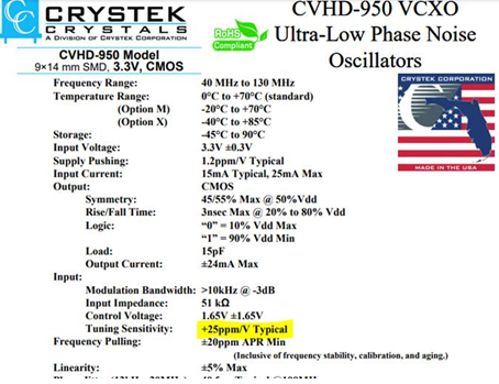
My primary requirement is to configure LMK04828 chip on board to take external 10MHz ref clock input and produce 245.76MHz to feed to LMX2594 chip which, in turn, is generating 409.6MHz. I did generate .tcs (and .txt) configuration file for the same and added the corresponding .txt file (i.e. LMK04828_245.76.txt) in xrfclk package in JupyterNotebook environment (path: /usr/local/share/pynq_venv/lib/python3.8/site-packages/xrfclk). Also, I am setting these clocks using command
xrfclk.set_ref_clks(lmk_freq=245.76,lmx_freq=409.6)

Now the problem is- My design is working even when I am not feeding the external clock to the board which means it’s definitely taking driving_clock from another input pin and I can’t figure out which one or there's something which I am missing here.

Could you please guide and help me resolve this issue?

Attached is my config file (.tcs) and hex register (.txt) file for reference and also some snaps which might be helpful for you to understand the issue more clearly. "

LMK04828_245.76 (1).tcs

LMK04828_245.76.txt
R0 (INIT)	0x000090
R0	0x000010
R2	0x000200
R3	0x000306
R4	0x0004D0
R5	0x00055B
R6	0x000600
R12	0x000C51
R13	0x000D04
R256	0x01006A
R257	0x010155
R258	0x010255
R259	0x010301
R260	0x010422
R261	0x010500
R262	0x010673
R263	0x010703
R264	0x01086A
R265	0x010955
R266	0x010A55
R267	0x010B00
R268	0x010C22
R269	0x010D00
R270	0x010EF0
R271	0x010F30
R272	0x01106A
R273	0x011155
R274	0x011255
R275	0x011301
R276	0x011422
R277	0x011500
R278	0x011673
R279	0x011703
R280	0x01186A
R281	0x011955
R282	0x011A55
R283	0x011B01
R284	0x011C22
R285	0x011D00
R286	0x011E72
R287	0x011F03
R288	0x012074
R289	0x012155
R290	0x012255
R291	0x012301
R292	0x012422
R293	0x012500
R294	0x012670
R295	0x012733
R296	0x01286A
R297	0x012955
R298	0x012A55
R299	0x012B00
R300	0x012C22
R301	0x012D00
R302	0x012EF0
R303	0x012F30
R304	0x01306A
R305	0x013155
R306	0x013255
R307	0x013301
R308	0x013422
R309	0x013500
R310	0x013673
R311	0x013703
R312	0x013800
R313	0x013903
R314	0x013A01
R315	0x013B40
R316	0x013C00
R317	0x013D01
R318	0x013E03
R319	0x013F02
R320	0x014009
R321	0x014100
R322	0x014200
R323	0x014331
R324	0x0144FF
R325	0x01457F
R326	0x01461B
R327	0x01470A
R328	0x014802
R329	0x014942
R330	0x014A06
R331	0x014B26
R332	0x014C00
R333	0x014D00
R334	0x014EC0
R335	0x014F7F
R336	0x015011
R337	0x015102
R338	0x015200
R339	0x015300
R340	0x01547D
R341	0x015500
R342	0x01567D
R343	0x015700
R344	0x0158C0
R345	0x015907
R346	0x015AD0
R347	0x015BDA
R348	0x015C20
R349	0x015D00
R350	0x015E00
R351	0x015F0B
R352	0x016000
R353	0x016119
R354	0x016244
R355	0x016300
R356	0x016400
R357	0x0165A0
R369	0x0171AA
R370	0x017202
R380	0x017C15
R381	0x017D33
R358	0x016600
R359	0x016700
R360	0x0168C0
R361	0x016959
R362	0x016A20
R363	0x016B00
R364	0x016C00
R365	0x016D00
R366	0x016E13
R371	0x017300
R386	0x018200
R387	0x018300
R388	0x018400
R389	0x018500
R392	0x018800
R393	0x018900
R394	0x018A00
R395	0x018B00
R8189	0x1FFD00
R8190	0x1FFE00
R8191	0x1FFF53

Please help to advise. Thank you for extending your support.

Kind regards,

Marvin

  • Hi Marvin,

    In the customer's configuration, CLKin0 should be the only clock source used by the device due to the CLKin_SEL_MODE configuration, so it is unlikely that another input is being passed to it. In the Holdover page I see that the holdover function is enabled and the device will attempt to maintain an accurate output in the event that PLL1 loses its lock (which would happen if CLKin0 was initially on but then shut off). This might explain what the customer is seeing. If this is not desired behavior, I recommend that they disable Holdover and see if it works as expected. If it's still somehow producing outputs with both inputs off and holdover off, we can take a look at their board design for more clues.

    Best,

    Evan Su

  • Hi Evan, 

    Thank you for your response. Please see the feedback from our customer.

    "I tried your suggestion- disabling holdover and disabling both the clocks still produce desired output i.e. I still get my design working.
    But I tried one interesting thing as a test to verify if it's actually running on an external clock- 
    1. Give an external 10MHz external reference clock to the RFSoC4x2 board (CLK_IN) and also connect another 10MHz output from the clock to the scope. 

    2. Connect the SMA cable from the unloaded SMA clock connection (OUT11 pin of LMK04828 chip) to the scope. (Frequency at this pin is set at 10MHz)  

    3. Compare these two inputs of scope and check if the clocks are drifting against each other. 

    Observation: They don't since both frequencies are locked.


    Disconnect the external clock from the board and now compare the two inputs of scope and check if the clocks are drifting against each other. 

    Observation: The waveforms drift against each other as their frequencies are not locked anymore.  

    Can you comment on this?" 

    Please help to advise. Thank you for extending your support.

    Kind regards,

    Marvin

  • Hi Marvin, here is my response for the customer:

    In the test case where you disconnected the external clock from the board, the relative drift of the external clock compared to the output indicates that they do not have constant phase, this means that the PLL should not be locked. You can confirm this by reading the lock detect pins or the RB_PLL1_LD/RB_PLL2_LD registers, let us know what you see.

    I have not worked much with the LMK04828 specifically, but most of our devices will still drive outputs when the PLL is unlocked unless the user specifically disables the outputs or removes power to the output drivers. Without holdover, this unlocked output will typically have an indeterminate frequency and phase and is considered invalid. Can you elaborate what you mean by the design working when the input clock is shut off? Is the LMX2594 is mysteriously producing a correct 409.6 MHz output?

    Thanks,

    Evan Su

  • Hi Evan, 

    Thank you for your response. Please see the feedback from our customer.

    "Yes, that's correct! When the external clock is not connected, PLL1 LED turns off (PLL2 LED is still ON) which indicates PLL is not locked, right?. 
    So, when I say design is working, I have shut down clk_1 which is driven by other on-board clock synthesizer (which I don't want); only enabled clk_0 (external clock SMA on RFSoC4x2 board) using .tics file configuration and even when I don't provide/connect external clock to the board, LMK04828 chip is (I think) mysteriously generating 245.76MHz (the frequency I have set at the output) which in turn drives LMX2594 chip to generate 409.6MHz. I haven't checked explicitly whether LMK04828 is generating 245.76MHz - I just assumed since everything is still working fine and my design didn't crash when I ran it on the board. Please guide me.
    Also, is there any way I can check these frequencies, maybe using the pynq framework? Having said that, these chips are enclosed in a case on the board to avoid interference so I do not have direct access to chip/pins."

    Please help to advise. Thank you for extending your support.

    Kind regards,

    Marvin

  • Hi Marvin, here is my response for the customer:

    That is indeed very strange. A couple of ideas for now:

    • Check if there is any activity on the OSCin pins, but that might be difficult if the chip and VXCO are enclosed. If PLL1 is unlocked but PLL2 is locked and holdover is fully disabled, then it should not be possible for PLL2 to lock onto any signal.
    • Turn the LMK04828's outputs completely off, so that it should not be sending any signal downstream, and see if your design crashes

    I have paged a device expert on this thread but he seems to be busy lately, I hope he can check in next week.

    Best,

    Evan Su

  • Hi Marvin,

    When there is no input at PLL1 (CLKin0/1 inputs are OFF) and the holdover is disable, the Vtune1 voltage (tuning voltage to VCXO) may jump to 3.3V or 0V (based on VCXO is used), which shift the VCXO frequency based on its tuning range.

    Consider the CVHD-950 VCXO (122.88MHz) used in LMK04828EVM, which has an tuning sensitivity +25ppm/V.

    Now, If the PLL1 goes unlock and Holdover is disable, the Vtune1 voltage jumps to 0V/3.3V and with 1.65V change, VCXO frequency will jump by 25*1.65 = 41.25ppm, which will be ~5kHz frequency drift on 122.88MHz output.

    For the LMK04828 lock detect accuracy, you can set the proper PLL2_WND_SIZE and PLL2_DLD_CNT.

    Thanks!

    Regards,
    Ajeet Pal