Part Number: CDCLVC1310
Hello
1、schematic check
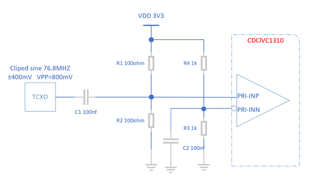
We use CDCLVC1310 as CLK BUFFER,The clock input and output circuits are shown in the following figure,please help check if the circuit is correct.
The detailed information of the circuit is as follows:
(1)TCXO VPP=800mV(±400mV),clipped sine ,frequency is 76.8MHZ,
(2)76.8MHZ is a single end CLK
(3) We connnected the clipped sine clock of 76.8MHZ to PRI_IN
(3)Need to convert clipped sine to LVCMOS(0~1V8)
2、In addition,About CDCLVC1310 ,I also have some question to ask for advice,
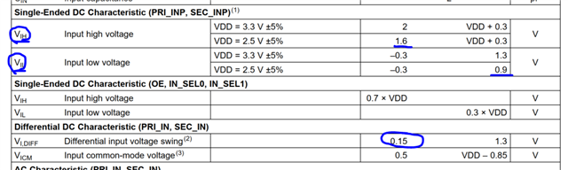
Single-end DC characteristic min( VIH-VIL)=0.7V,so how dose the chip achieve wing of 0.15V.