Hi TI team,
Since I am very new to use clock generator IC's, the following queries came into my mind.
Can you please clarify following my queries on CDCE6214WRGERQ1.
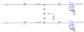
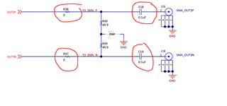
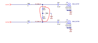
1. When I saw EVB schematic of CDCE6214WRGERQ1, I have observed that OUTx_P & OUTx_N lines contains a series 0ohm resistor and 0.1uf capacitor connected .
Whether these are mandatory to implement in designs. If answer is yes, may I know the reason for using 0ohm resistor and 0.1uf cap.
Majorly the role of 0.1uf capacitor I would like to know.
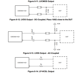
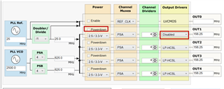
2. OUT1_P & OUT1_N can be used as LVDS-like/LP-HCSL/LVCMOS Output.
In EVB of CDCE6214WRGERQ1 OUT1 channel does not contains series capacitor, is this configured only for LVCOMS purpose in EVB ? please confirm.
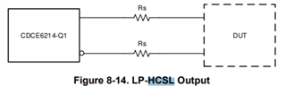
If we want to use OUT1 channel as LVDS-like/LP-HCSL, de we need to add series resistor and series captor as like OUT2 & OUT4 channels in EVB? Please confirm.
3. Can we use single 100ohm resistor across OUT_P & OUTN channel, or we need to provide split termination as per CDCE6214WRGERQ1 EVB ( 2 x 49.9 ohm and 0 ohm option to GND)
If answer is split termination resistors (2x 49.9 ohm) , may I know the reason.
4. CDCE6214TWRGETQ1 IC unused OUT_P & OUT_N channels can we left open or tie to a test point ?
If answer is No, please suggest termination process for unused OUT_P & OUT_N channels.
Thanks & regards,
Murali penta.