This thread has been locked.

If you have a related question, please click the "Ask a related question" button in the top right corner. The newly created question will be automatically linked to this question.

LMX1204: SPI INTERFACE INCONGRUENCE WITH LMX1204 EVAL.

Part Number: LMX1204

Hi Team,

We use yours component LMX1204 in a custom PCB board. We encountered some difficulties in the SPI Programming signals (SCLK,SDO,SDI & CS).

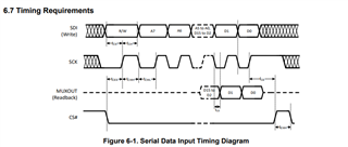
In the Figure 6-1 of the datasheet that is illustrated below, the SPI is defined (also in the text following the figure in the datasheet "Recommended SPI settings for this device are CPOL=0 and CPHA=0.". This means, like the figure below that the first edge of the SCLK after the CS# is a rising edge, and the clock pin when there are no SPI cycles performed is low. Also the Datas on SDI and SDO are sampled on the rising edge of the clock and "changed" on the falling edge.

Since we can't program the LMX1204 on our custom PCB, we perform different analysis and since we have bought also the LMX1204 eval board we measure the SDI,SCLK and CS# on the pins provided on the eval board.

I will show the oscilloscope signals on the board in the figure below.

It seems like the CPOL is not 0 but 1, since the first edge of the SCLK is falling after the CS#. I will zoom it for you:

The yellow plot is the CS, the violet the SCLK and the blue the SDI. 

We use the TICS PRO SW interface to program the LMX1204 Eval board. 

Can someone explain me why there is this difference between the Datasheet and the operation mode used on the Eval Board?

Thank you very much, 

Best regards!

  • George,

    So it sounds like the EVM is programming fine, but the manner it is doing so is inconsistent with the statement "CPOL=0 and CPHA=0"

    After the CS# goes low, the data is clocked in on the rising edge of SCK.

    From my understanding of SPI:

    CPOL = 0 means that the clock idle state is low

    CPHA=1 means that data is sampled on the leading (First) clock rising edge

    So from your measurement, indeed, it seems that CPHA = 1, but CPOL =1 as the clock idle state is high, not low.

    We have other programming software that would have the idle state of clock to be low and this works also.

    So are you suggesting that we should say the following?

    CPHA = 1

    CPOL can be 0 or 1

    Regards,
    Dean

  • Hi,

    Thank you for your reply, i appreciate that. Is all correct what you say, 

    I only need to reply at this:

    So are you suggesting that we should say the following?

    CPHA = 1

    CPOL can be 0 or 1

    We've try to program the LMX1204 with CPOL = 0 but this for us not works. So we do a HW connection from ours LMX1204 to the pins SDI,CS and SCK of the Evaluation board. This worked very well.

    So my doubt is that the CPOL = 0, specified on the datasheet for this component is wrong. 

    Can you verify internally what is the correct SPI settings in order to program the LMX? 

    Thank you very much,

    Best Regards!

  • Hi George, 
    Dean will get back to you as soon as he can!

    Regards, 

    Vicente 

  • For our devices, we have programmed in the manner as shown in our datasheets with the clock both staying high and staying low after program and had sucess.  Our older software used to program this way, but TICSPRO seems to keep SCK high after programming.

    As in both cases, the SCK goes low during programming and we know it works for the CPOL=1 case, it is hard to envision that if SCK was held high or low at some other previous period in time would prevent it from programming.  So I think that it is more likely the case that even with CPOL=0, the device is responding to programming, but there is some other factor not considered.  For instance, if SCK is high, then we know that there is nothing programmed during this time.  But if SCK is low, then potentially there could some glitch on the line that clocks in an erroneous bit.

    I am no micocontroller expert, so I don't know if CPOL=0 vs 1 has any other impact other than the SCK line being low after programming.  Our SPI read/write speed in the datasheet is 2 MHz, so there could be some kind of timing issue involved.


    Regards,
    Dean

  • Hi Dean,

    Thank you for your reply. I understand your point of view about this question. I have however some more doubts, in particular:

    Our SPI read/write speed in the datasheet is 2 MHz, so there could be some kind of timing issue involved.

    If the 2 MHz is the right frequency, why about the Tcwh and Tcwl that are both expressed as max value of 100ns (this means 200ns of period so Max Frequency is 5MHz). I measure also the SCK frequency of the LMX1204 Eval. Board and that is equal to 125KHz. 

    We use also the SPI of CPOL = 1 and CPHA = 1 with a SCK frequency equal to 125KHz. But i encountered the same problem and i fail to program the component.

    I have also a new question about the TCES. I interpret this time as the time between the falling edge of the CS and the first valid clock edge (for CPOL = 1, the first falling edge). In the Datasheet is reported the Max time 20ns, is possible that this can be the minimum time? On the Eval. board the time measured is circa 500ns. How much this time can be relevant in the correct programming sequency of the component? There is an interval (min-max) to respect?

    Thank you so much,

    Best Regards!

  • With the exception of the first spec, these should all be min specs;  that's a pretty big datasheet blooper.

    These digital timing specs have some good margin in them and the way we typically test is run some digital patters for a go/no go test.  We typically don't do a breakpoint test where we find the limit where the part actually starts to fail.

    With 125 kHz write speed, it seems hard to blame this as a pure timing spec.

    For TCES, your interpretation is correct.  

    For these timing specs, my thought was if there was an issue, the symptom would likely be that either miss or get an extra clock.  

    But lets have a thought experiment about what happens with CS# and SCK low and some noise.

    Suppose you program a register and then latch it in and then SCK and CS# are low.  Now suppose there is an unwanted clock pulse on SCK due to some unwanted noise.  So one bit gets clocked in.  Now you start clocking in the next register, but you already have one big clocked in, which would be the read/write bit.  Then you clock the rest in, but everything, including the address is shifted by one bit.  On the next to the last bit, the part sees that you have clocked in all the data, so it automatically latches it into the register.  Then the last bit gets clocked in as the next register.  Then CS# goes high and clocks in 1 bit.  So a mess.  But if you have SCK high, then it prevents an erroneous clock pulse from happening

    So what I am wondering is if programming is not working and is completely being ignored, or if you are actually programming the device, but with not the information you intended.

    Regards,
    Dean

  • Hi Dean,

    Thank you for your response. I will reply at some points of your discussion.

    With the exception of the first spec, these should all be min specs;  that's a pretty big datasheet blooper.

    Ok, perfect. It also need to be changed the min values of time. Since frequency is max 2MHz, the pulse widths of clock needs to be changed.

    For these timing specs, my thought was if there was an issue, the symptom would likely be that either miss or get an extra clock. 

    Your symptom is also correct. Analyzing better the SPI trace of the LMX1204 eval board, we've noticed that the SPI number of SCK's are 24, that means if the data is 16 bit, 1 bit for R/W, this means that the address in 7 bits for a total of 24 clock cycles.

    In the Figure 6-1 of the datasheet is illustrated the SPI interface that is composed by 1 bit R/W, 8 bit Address and 16 bit Data, for a total of 25 SCK cycles.

    We also implement the CPOL = 1 and CPHA = 1 in order to maintain the same guideline of the Eval Board.

    Changing the Address from 8 bits to 7 bits we can program the device, that works fine and also allows me to readback the register values. So at the end, is correct with 7address bits and 1bit R/W + 16t bit Data & CPOL = 1 and CPHA = 1. I've put there a screenshot of the correct trama:

    Write operation: 

    Read operation: 


    Thank you so much,

    Best Regards!!


  • George,

    OK, another datasheet blooper ...

    The address is actually 7 bits, not 8, so the diagram is wrong.  There is a R/W bit.  So sometimes we are careless and consider the R/W part of the address, but it is not.  But it should be 24 bits.

    So the datasheet was telling you to send 25 bits and it sounds like you were doing this.  But by keeping Data high, it caused a happy coincidence as it canceled this unwanted address bit.  So it seems like the two issues in teh LMX1204 datasheet are:

    1. Specs swapped in the min/max column

    2. Timing diagram should show R/W bit + 7 address bits, not 8 address bits.

    Regards,

    Dean

  • Dean,

    Exactly! Thank you for your professionality!

    Regards,

    -George

  • George.  Thanks for pointing these things out. We will update the datasheet.

    I will close this thread.