Hi ,
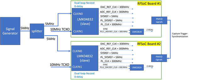
I am currently using the below setup to achieve the multi-board multi-tile synchronization.
I am using a splitter to feed 5 MHz into both RFSoC Boards as shown below. I have used the registers for LMK04832 and program onto both RFSoC boards but could not get the Multi-board clock synchronized. Attached is the tcs file and registers.
1) Checked Status_LD1 pin and it seems that PLL1 is not locked. Why?
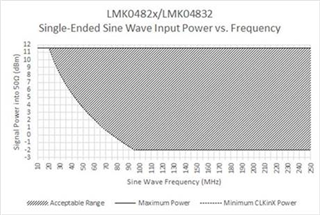
2) What configurations do we set to make sure that the LMK04832 takes only external clock to achieve MB MTS ? The external clock 5MHz will feed into CLKIN0 of the LMK04832 slave boards.
R0 (INIT)	0x000090
R0	0x000010
R2	0x000200
R3	0x000306
R4	0x000463
R5	0x0005D1
R6	0x000670
R12	0x000C51
R13	0x000D04
R256	0x01000A
R257	0x010108
R258	0x010260
R259	0x010344
R260	0x010420
R261	0x010500
R262	0x010601
R263	0x010711
R264	0x01080A
R265	0x010908
R266	0x010A00
R267	0x010B44
R268	0x010C20
R269	0x010D00
R270	0x010E01
R271	0x010F11
R272	0x01100A
R273	0x01110A
R274	0x011200
R275	0x011344
R276	0x011420
R277	0x011500
R278	0x011601
R279	0x011711
R280	0x01180A
R281	0x01190A
R282	0x011A00
R283	0x011B44
R284	0x011C20
R285	0x011D00
R286	0x011E01
R287	0x011F11
R288	0x01200A
R289	0x01210A
R290	0x012200
R291	0x012344
R292	0x012420
R293	0x012500
R294	0x012601
R295	0x012721
R296	0x01280A
R297	0x01290A
R298	0x012A00
R299	0x012B40
R300	0x012C00
R301	0x012D00
R302	0x012E01
R303	0x012F11
R304	0x01300A
R305	0x01310A
R306	0x013200
R307	0x013344
R308	0x013430
R309	0x013500
R310	0x013601
R311	0x013701
R312	0x013820
R313	0x013900
R314	0x013A02
R315	0x013B58
R316	0x013C00
R317	0x013D08
R318	0x013E03
R319	0x013F0D
R320	0x014009
R321	0x014100
R322	0x014200
R323	0x014351
R324	0x014480
R325	0x014500
R326	0x014618
R327	0x01470E
R328	0x014802
R329	0x014942
R330	0x014A03
R331	0x014B06
R332	0x014C00
R333	0x014D00
R334	0x014EC0
R335	0x014F7F
R336	0x015001
R337	0x015102
R338	0x015200
R339	0x015300
R340	0x015401
R341	0x015500
R342	0x015601
R343	0x015700
R344	0x015896
R345	0x015900
R346	0x015A01
R347	0x015BD4
R348	0x015C20
R349	0x015D00
R350	0x015E1E
R351	0x015F0B
R352	0x016000
R353	0x016101
R354	0x01624C
R355	0x016300
R356	0x016400
R357	0x01650F
R361	0x016958
R362	0x016A20
R363	0x016B00
R364	0x016C00
R365	0x016D00
R366	0x016E13
R371	0x017310
R375	0x017700
R386	0x018200
R387	0x018300
R358	0x016600
R359	0x016700
R360	0x01680F
R1365	0x055500