This thread has been locked.

If you have a related question, please click the "Ask a related question" button in the top right corner. The newly created question will be automatically linked to this question.

LMK04832: Recommended design for power input of VCC7, VCC8, VCC9

Guru 11220 points
Part Number: LMK04832
Other Parts Discussed in Thread: ADC12DJ3200, , ADC12DJ3200EVM,

Hello,

My customer is using LMK04832 to provide main clock and SYSREF clock to ADC12DJ3200.

They designed the power inputs of VCC7~9 of the LMK04832 as follows in the same way as the ADC12DJ3200EVM circuit.

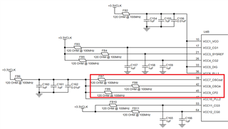
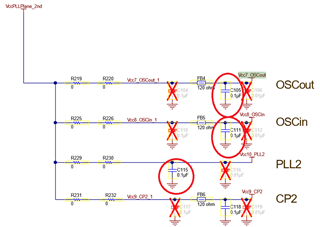
Recently, they found that capacitors were added to the VCC7~9 power input of the LMK04832EVM, unlike the ADC12DJ3200EVM circuit.

Q1) What is the role of the above capacitors?

Q2) Is the use of the above capacitors mandatory?

Q3) Is ADC12DJ3200EVM's LMK048xx circuit wrong? Or did you remove the capacitors for some other purpose?

Thank you.

JH

  • JH,

    Q1) Each cap powers some relevant circuitry within the device, as expected by the name:

    • OSCIN supply powers the OSCIN clock buffer path
    • OSCOUT supply powers the OSCOUT/CLKIN2 clock buffer path in both directions
    • PLL2 supply powers the divider and state machine circuitry for PLL2, as well as all the internal VCO calibration logic circuits
    • CP2 supply powers the output of the charge pump

    Capacitors on these nets would act as bypass capacitors and as loop stability impedances for the LDOs within the LMK04832. Depending on how much current at these pins can fluctuate moment-to-moment, and upon the frequency profile of that fluctuation, these capacitors may be useful, or unnecessary.

    Q2) Their population depends on whether the circuit uses those features, and whether the bypass capacitance provides any meaningful value in those cases. The default use case for the ADC12DJ3200 puts the LMK device in a clock distribution mode, in which the relevant portions of the circuit are mostly powered down because PLL2 is inactive. Technically it looks like the OSCin/OSCout supplies are used for buffering a 100MHz source... but the bond-wire inductance from the die to the supply pin is high enough that any changes in current would be sourced through on-chip bypass capacitance rather than external bypass capacitors at 100MHz. Note that if the reference were a lower frequency, e.g. 10MHz, then bypass capacitance on OSCin/OSCout supplies could plausibly provide some benefit, since the bond-wire inductance would no longer be the constraining factor in the net impedance.

    Q3) Given that the ADC12DJ3200EVM uses 100MHz XO on OSCin/OSCout, and uses the LMK04832 in distribution mode in which PLL2 is unused, I think the ADC12DJ3200EVM can correctly omit bypassing on these nets. However, if an evaluation user wanted to use LMK04832 PLL2, or replace the XO with a lower frequency device, they would want to insert the same bypass capacitors as the LMK04832EVM.

    Regards,

    Derek Payne