


Part Number: LMK1D2108
Other Parts Discussed in Thread: LMK1D1208
I'm using the LMK1D1208 as LVDS buffer in my design. I'm measuring on the hardware and noticed that the 8 outputs coming from IN0 are giving the inverted logic level. When a logic '1' is at the input (P-N voltage is >0), a logic '0' comes out (P-N voltage is <0) and vice versa.
The 8 outputs coming from IN1 are giving the same logic level.
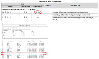
For IN0 the datasheets says IN0_P = pin 9 and IN0_N = pin 10
But in the IBIS model I see that IN0_P = pin 10 and IN0_N = pin 9. And this also corresponds to the behavior I measure on my hardware.
Can you confirm that there is a mistake in the datasheet and that the pin numbering in the IBIS model is the correct one?
Thank you.
