This thread has been locked.

If you have a related question, please click the "Ask a related question" button in the top right corner. The newly created question will be automatically linked to this question.

LMX2581: not achaive proper frequency and no digital lock

Part Number: LMX2581
Other Parts Discussed in Thread: LMK04906, , CODELOADER, USB2ANY

Hi.

In project we have using two LMX2581 in one PCB, both are the the same circut, role, and very similar layout. On the other hand, layout doesn't differ significantly from EVM board. Both have OSCin signal distributed by LMK04906 with frequency 100MHz, and amplitude about 1,6Vpp (on OSCin pin), is good looking suqare wave. Desing circut, in loop filter section is similar as in 9.2.2.2 chapter in datasheet. Our target is to acheive output frequencies from 1-2GHz (1000G, and 1500G for example), on one output of each chip. We use TICS Pro to generate register values, and write it by SPI using Raspberry Pi. Programing sequence of LMX2581 contain: program R5 with RESET bit, program registers R15-R0 with about 500us delay between each register, and again program R0 after about 160ms. Chips are programmed each time in sequence: LMK, LMX(1), LMX(2), so i can observe beachvior on two LMX because each get the same cofiguration. DIfference is one: LMX(1) has AC-coupling capacitor in OSC signal near the LMK, but LMX(2) has additional capacitor directly before OSCin pin (to do the circut identicaly like EVM board).  Clock from LMK04906 is still present, but chips are on the same board. 

I tried to achaive target output frequencies, but when it get unsuccesfull i tried to get any set frequency and get lock status. I tried several dozen configurations, and can't achaive proper frequency, and get "DLD & Vtune Good" on LD pin. In some cases device gives maximum VCO freqency, eventually divided by VCO_DIV. In other configurations the frequency is wrong, but not like extreme of VCO, and sometimes differs between two programming sequences with the same config. In some configurations device gives frequency differs from config (example: set 1900M, get 2200M, or 2050M), but i get "Vtune" on LD pin (good sign :) ) and Vtune voltage is stable about 1,26V, what mean (as i readed from other topics) that the voltage tuning is OK, and analog part is propoerty locked, but i cant get the "DLD" (Digital Lock Detect). In some configs i get 1810MHz, when set 1805MHz, what looks good, but any lock occurs, deviation is 3MHz, and changing set frequence down to for exampe 1750MHz, i get 1900MHz.  Now i put more hope in LMX2581 with additional capacitor on OSCin pin, because it always set the "OSCin Det" on LD, when LMX with no additional capacitor set it sometimes. I tried to: changing VCO (by force), pump gain, dividers and multiplers combinations, VCO_CAPCODE values, Fpd frequency, changing programing sequence (for example adding 3 times programmming R0 and sometimes it changes effects) and some others and cant get it. I see that the highest Fpd frequency is better (as described in datasheet) but not always. I tried to use LD pin as "R/2", or "R/4", but in some cases i did not get this signal on LD pin. Output frequencies has deviations about 1-3MHz. Sometimes i see that the frequency is proper for a fraction of a second after programming, and change to unproper. I have some questions about diagnostic functions, and of course main question:

1. How to get proper frequency and lock? How can i debug, or diagnose it?

2. Can i interpret "OSCin Det" on LD pin as the OSCin signal is proper? Information in datasheet mean that i can't.

3. How can i check that 4 important things was right: programming, input signal, voltage lock, digital lock?

I think is the digital (phase detector) issue, but as i think if the Vtune voltage is proper, we need just phase detection, but i don't know how to diagnose/debug it. 

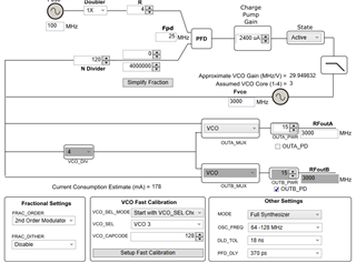
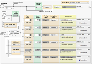
Now i back to starting point (9.2.2.2 chapter config from dataseheet). Set config as below, and get freqency as below ( on LMX2581 with additional capacitor on OSCin pin, because without it, the second LMX gives 2800MHz), "Vtune" high on LD, and Vtune voltege 1,23V.
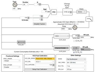
I would be very grateful for your help.

Best regards

  • Hi There,

    Please use a spectrum analyzer to verify the output frequency of a synthesizer. The scope will not provide accurate frequency information.

    There are several problem in your configuration.

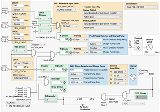
    you have set MASH_ORDER to Integer but your fractional numerator is not zero. The fraction will eventually be ignored so the output frequency will be 25MHz x 119 = 2975MHz.

    2975MHz or 3000MHz requires VCO3, but you have force the chip to use VCO1, it will definitely not lock.

    Here is an example to output 3GHz.

  • Hi, thanks for really quick response.

    Sorry, i have no saw this simple mistake with forcing VCO in the graphics i add to topc, but before start topic i tried amount of time the configs, without forcing VCO.


    In my config:
    -I disabled forcing VCO, and choose start with VCO1 - no changes.
    -Changed FRAC_ORDER to: 1nd, 2nd, 3nd - no changes. I mean You mean FRAC_ORDER, cause i can't find MASH_ORDER (In TICS, or in datasheet).
    But by the time of test, about several minutes, output frequency changes from 1900M to about 2000M.

    I tried config from Your graphics, but output frequency is about 2930-2960MHz, changing start VCO to VCO1,
    or forcing VCO3 doesn't effect. In all above cases Vtune (LD pin) is set high.

    Stragne is that i have no R/4 signal on LD pin (of course is configured as R/4), when i have OSCin signal,
    and "OSCin Det" on LD pin set's high - of course not simultaneously. Programming looks OK, but changing some single bits in config
    makes associated changes in the device behavior. So i think i can't be sure that the device see the proper input OSCin signal. But in some config (i have no saved it) the signal on LD pin (in R/4 mode) ocurs, but results of setting proper output frequency and lock was the same. What is proper way to searching the issue reason? I think in first step i schould check that device see proper OSCin signal, and check that programming is proper, but how to be sure for example about first one for 100%.

    Have You meabe the the least demanding  example to try? For example for output frequency 1GHz, and 1,5GHz? 

  • Hi There,

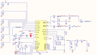
    Could you provide the schematic?

  • Hi There,

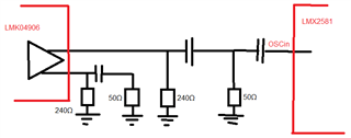
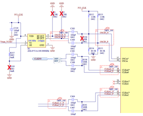
    Your T-pad at OSCin has 15dB loss, what is the purpose of this design?

    The connection between LMK and LMX device should be as follows:

    You should get 800mV signal at the 50Ω resistor at OSCIn, check this with a scope.

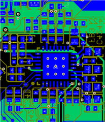
    In your layout, I assume there is a solid ground plane below the blue layer?

    The green layer should also be shielded with a solid power/ground plane.

  • Hi, thanks.

    Design is directly taken from datasheet, which contain layout example too and is similar within OSCin signal.

    Before circut edition i get output frequency about 1972MHz, Vtune LOW, Vtune voltage 3,3V, and only high state on R/2. So i edited connection between LMK-LMX as You suggest, and i have about 1Vpp 100MHz clear sine wave on 50Ohm resistor at OSCin. I used standard Rigol scope, with measurement range to 100MHz, but when i use R&S scope with range to 8GHz, and input impedance 50Ohm i takes about 4,5Vpp square (but i think is wrong/unproperty method). I used config from Your graphics, and output frequency is about 2935MHz, Vtune is LOW, and Vtune voltage is about several mV, but R/2 signal is OK. For just try i changed starting VCO to VCO1 and frequency changes to about 1900MHz, and again i change it to VCO3 and now frequency is about 3010MHz, with about 11MHz deviation i cant change it a little bit by changing for example N Divider.

    Yes, layers are in order: signal(blue) - solid ground - ground/power - signal(green) - solid ground - ground/ power - and 4 other layers.

    Can You tell me what value of input (OSC) signal will be interprett by device as valid (i don't mean range, but valid)? 

    And the timing when programming is performed is critical, or may have impact on proper device VCO calibration? I mean i have about 164ms delay between programming R5,R15-R0 and again R0, and 170-500us delay between each single SPI frame, which occurs in my application.

    Fun facts:

    - Programming this LMX with config files which i crated before, which contains different target frequencies gives still about 3010MHz - programming is proper, because values like a amplitude changes in order to config. Channel divider doesn't work - when i enable it, just signal distortion occurs.

    - Second LMX on the PCB have no input signal but still set Vtune voltage to 1,26V and max of VCO4 frequency on output.

    I looked ad pin to pin replacement/newer design chip, but i can't find it Your offer. I use LMX2581S, but i find LMX2581E - is some significant difference between them?

    You think the problem is related more with: input signal, layout, supplies, config, programming, or loop filter?

  • On the end of the day after several dozen programming sequences, for try i added 50MHz oscillator with CMOS output as source for OSCin of second LMX, with circut from another topic (graphics below).

    I used Your config for first LMX, and the same config with changed OSC frequency to 50MHz for second LMX, and as i saw, the frequency changes on both LMXs: both have max VCO4 frequency on outputs - about 3800MHz. Signals on R/2 was right, Vtune is NOK.

  • Hi There,

    There is nothing wrong with the configuration, we can get it lock to 3GHz with a 100MHz input.

    TICS Pro configuration file.

    3GHz output.tcs

    OSCin only needs 400mV signal, if you can confirm you see 800mV square wave signal, then hardware is fine. 

    Check to see if this is a software issue. Capture the SPI signals to cross check you have programmed it correctly. 

  • Hi, thanks.

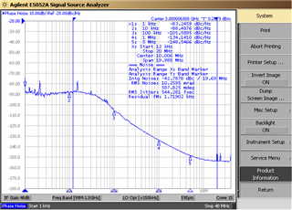
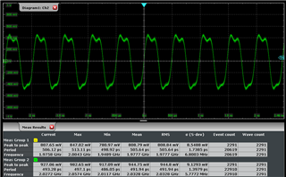
    Please send me capture of SPI signal from Your application (Codeloader), i want to see timing details. I use KingstVIS logic analyzer but i will be satisfied if You send me just screens (from analyzer, not datasheet)  which shows writing to about two/three registers (8 SPI frames minimum) with marked timings, or time scale/div. And the timing between writing main config and again writing R0. Chip select pin state is needed too. Because i changed something in software and with Your configruration i get right 3GHz, and "DLD&Vtune Good" OK, and i can change frequency in config and device still show DLD, and Vtune lock, but to some range. For example the 2,8GHz, or 3,05GHz is available, because measured frequency isn't equal - error is about 0,0012GHz (graphics below for 3,05GHz). Meabe this is error of my measurement, because i use scope with FFT, not direct spectrum analyzer (if it may made difeerence).

    When i try to get one of my two target frequencies - 1530MHz but LMX gives about 2,5GHz and show DLD, and Vtune lock, so i will be trying with communication software, but i need the graphisc which i described above. You can send me working (in Your set) config for 1070MHz and 1530MHz - i will try it. 

  • Hi There,

    If you were using my .tcs file and you could get it lock to 3GHz, there is no SPI communication issue.

    When you change the output from 3GHz to 1530MHz output, what did you program?

    FYI, you should program:

    R5: 0x0030 8805

    R0: 0x6099 0000

    R3: 0x2000 F3E3

  • Hi, thanks.

    Changing the values as You suggest gives 1912,47MHz in TICS Pro, but it doesn't matter, but:

    I made some newer changes in software (config writing), and changed cfg just in the N Divider and Fractional area to take my target frequencies, and it works.

    So i think the LMX2581 SPI controller has some critical timing dependencies. That's why I asked you for screenshots of SPI communication with a time division.

    Next question is about accuracy of frequency:

    When I reset the LMX (via the CE pin) again and again and upload the configuration, the output frequency differs from the set one (1530MHz) by about 2kHz, but when I increase the interval between resets to several minutes, the frequency could differ by 10kHz, 28kHz, 80kHz, 120kHz. This difference does not change after LMX is latched (DLD & Vtune Good). Can You tell me what the difference depends on?

    I have one question about LMK04906 too: I have enabled 4 outputs, on 3 of them i have almost target signal, but on forth one, the signal is present just several dozen ms when configuration writing occurs, and has wrong frequency (enaught high amplitude). Looking at the chip internal structure, i think that issue looks like just output circut problem, but its work enaught to give signal, so it doesnt look like significant damaged. It's meabe something like the some internal signal path after registers reset goes direct to output, but after configuration, the target (damaged) circut is enabled. I have this issue on two LMK, on the same (CLKout0) output, but CLKout0 and CLKout1 have the same external circuts (CLKout1 works good).

  • Hi There,

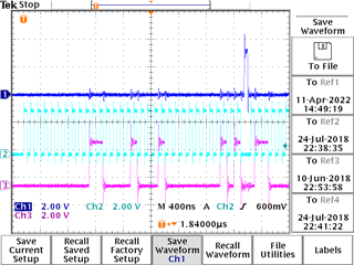
    Here is the SPI waveform, speed is 20MHz. There is no wait time between register.

    CE pin is not a reset pin. When CE = LOW, the chip is powered down. When CE resumes to HIGH, PLL will automatically lock to the last programmed frequency. However, internal LDOs need some time to settle down after the chip is recovered from power down. As such, the output frequency may not be accurate right after CE turns HIGH. The time taken for the LDOs to settle down is longer if the powerdown time is longer. 

    What output format did you program for LMK output? which output?

  • Thanks for graphics.

    I used CLK like 30-125kHz, but frequency didn't play a role.

    CE was low by about several dozen ms, and LMX was programmed about several second after CE goes high, so thats probably enaught time to establish and stabilize proper voltages by LDO's. I will look for furtcher results.

    Output format - what did You mean? I exported registers values from TICS Pro, register R0 is repeated at the beginning, because contains RESET bit set.

    I use outputs CLKout0 to CLKout3, and on CLKout0 i have no signal. 

    Thats my example cfg.

    R0  0x80160200
    R0	0x00140180
    R1	0x00140181
    R2	0x00140042
    R3	0x001400C3
    R4	0xC0140084
    R5	0x80140C85
    R6	0x06640006
    R7	0x01110007
    R8	0x04010008
    R9	0x55555549
    R10	0x9102412A
    R11	0x3401100B
    R12	0x130C002C
    R13	0x3B02002D
    R14	0x0200000E
    R15	0x8000800F
    R16	0xC1550410
    R24	0x000000D8
    R25	0x02C9C419
    R26	0xAFA8001A
    R27	0x18000C1B
    R28	0x00400C1C
    R29	0x0280019D
    R30	0x0100019E
    R31	0x0000001F
    

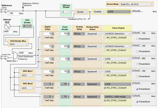
     I will be very gratefull if You send me test config for LMK04906, for following target:

    Input:

    - VCXO 100MHz on OSCin

    - CLK signal 100MHz on CLKin0

    Output:

    - CLKout0 100MHz LVCMOS(Norm/Inv)

    - CLKout1 100MHz LVCMOS(Norm/Inv)

    - CLKout2 480MHz LVDS

    - CLKout3 160MHz LVDS

  • Hi There,

    I created a configuration for LMK04906.

    6646.HexRegisterValues.txt
    R0 (INIT)	0x80160140
    R0	0x00140300
    R1	0x00140301
    R2	0x001400A2
    R3	0x001401E3
    R4	0x80140144
    R5	0x80140145
    R6	0x06640006
    R7	0x01110007
    R8	0x04010008
    R9	0x55555549
    R10	0x9102412A
    R11	0x0401100B
    R12	0x1B0C006C
    R13	0x2302826D
    R14	0x0200000E
    R15	0x8000800F
    R16	0xC1550410
    R24	0x00000058
    R25	0x02C9C419
    R26	0xAFA8001A
    R27	0x1000191B
    R28	0x0020191C
    R29	0x0180019D
    R30	0x0200019E
    R31	0x001F001F
    

  • Hi, thanks.

    Now i can't check that the LMK is latching proper (another hardware issue), but i will check it tommorow and I'll let you know because I think we're close.

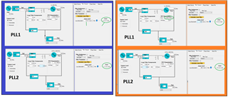
    But first i changed loop filters, like on graphics below: blue - previous, orange - actual. I use maximum loop bandwidths. Can You tell something about this values? I have VCXO with +/-50ppm pulling range, that gives 10kHz badwidth, but maximum PLL1 loop bandwith is 200Hz - it's not a problem?

  • Hi There,

    Loop bandwidth depends on your application.

    If the input clock to PLL1 is noisy, we should set a smaller PLL1 loop bandwidth, e.g. 10Hz. 

    For PLL2, which is used to generate high frequency clocks, since its input clock (VCXO) is clean, we should use a wide loop bandwidth to reduce the phase noise and jitter. In the LMK04906 EVM, we used 132kHz loop bandwidth.

  • Now i made some changes in LMK config, and i get just PLL2 DLD, but output frequency differs 10kHz from target 100MHz, this error is stable. For first i changed input source selection for PLL1 - in Your config it is CLKin1, but i need CLKin0 - or i understand something in wrong way.

    LMX's which are clocked by LMK get PLL DLD, but output frequency differs 100kHz for one of them, and 200kHz for another, from target 1070MHz, and 1530MHz. What is strange, that when i set PLL2 phase detecetor frequency to proper 100MHz, on PLL2 R/2 LD pin i get signal which i can't measure with my Rigol (i think is too high frequency), and PLL2 DLD doesn't occurs, but when i changed it to 50MHz (what is unproper, but it causes all outputs to 2x lower frequencies) i get 100MHz signal on PLL2 R/2 LD pin, and get PLL2 DLD. Vtune voltage when DLD occurs, is about 1,13V. PLL1 Vtune is about 0V, so it's look like tuning circut doesn't work, but when i changed charge pump polarity it goes to 3,3V so it is working, and on scope i see some tuning trying when configuration is writed, but it fails.

    I made some different config, focused on to lock PLL1. I restored 100MHz PLL2 phase detecetor frequency, and enabled EN_PLL2_XTAL.

    Now i see that the PLL1 DLD is high, but its randomly often gets low for several us. PLL2 DLD doesn't occurs. Vtune PLL2 is 3,3V, and Vtune PLL1 is 1,6V, and jumps up randomly often for several us, to about 3,3V and in this time PLL1 DLD goes low. But how get both PLLs lock :D

    In both configuration (which most significant change i see is EN_PLL2_XTAL) when i'm trying to measure VCXO output signal its It seems to disappear for brief moments when tuning occurs. Not tuned VCXO gives 100MHz with stable error about 10kHz. Signal doesn't look soo preety, but if i can get the R/2 signal, that mean i have proper OSCin signal - meabe i'm wrong. But i can see the negative effect of the presence of the measuring probe and it may be just its fault. VCXO signal is directly connected to OSCin, just by the AC coupling capacitors.

    I have important question:

    1. U use external VCXO, as OSCin for PLL2 - should i enable EN_PLL2_XTAL? As i undestand the datasheet i should enable it, because i'm not sure in 100%, because description is short, and i don't saw it enabled in Your config, or in EVM configs. It's look like it was nesesary to tuning the VCXO.

    I will be trying in next week, but all Your tips will be precious.

  • Hi There,

    If you use VCXO, you do not need to set EN_PLL2_XTAL bit.

  • Hi, thanks.

    I measured VCXO frequency when LMK is tuning it, and its 100MHz slided 10kHz down, or up if i change phase detector polarity. I made some strange LMX's config, where take into account this error/off-set and i get my proper frequency with error below 200Hz, but when the PCB temperature changes, it cause VCXO frequency change, and of course LMX2581 frequencies changes. But i know it's not proper way.

    VCXO takes edgy frequencies (100M + or - 10kHz), PLL1 is not locking, so it's look like overtuning. What i can do to stabilize it?
    I tried to change PLL1 loop filter bandwith to 100Hz, and change Kvco to default 0,0025MHz/V but no results. Kvco for my ASG-P-V-A-100.000 (VCXO) is 0,0082MHz/V what i calculated and used in previous PLL1 loop bandwith design (i use PLLatinum Sim). First what i thinked that if Kvco is too low, it may cause overvtuning on CP out/Vtune.
    CLKin0 signal looks well, is just abut 150Hz miss, and it comes from FPGA on another PCB, so has no strong temperature dependecies.

    So my questions:
    1. How can i stabilize it? It's just PLL1 loop filter issue? What i should focus on?
    2. What is output frequency accuracy for LMX2581?

    And i have some strange thing in config: I had target output frequencies set but PLL2 would not latch and when I changed PLL2 phase detector frequency to 2x lower it also reduced the output frequencies (i do not corected it), and after this change PLL2 locks, and i get proper target frequencies on chip - looks like TICS Pro bug? 

    That's my CLK and OSC circuit for LMK04906. 

  • Hi There,

    Differential CLKin should be AC-coupled, your schematic has all CLKin DC-coupled. 

  • Hi.

    I don't undestand - i see series capacitors in CLKin paths. I looked to datasheet and tried to remove termination resistor "after" capacitors, and give it "before" as datasheet commanded - no change. 

    I checked CLKin0 signal by "asking" LMK chip:

    - PLL1R on LD pin gives 1MHz - proper

    - CLKin0 Selected on Status_CLKin0 gives HIGH state - proper

    - CLKin0 LOS on Status_CLKin0 gives LOW state - proper

    I checked OSCin signal in the same way:

    - PLL2R/2 on LD pin gives 50MHz - here is some strange: in config i have PLL2 phase detector frequency as 50MHz (and all output frequencies 2x lowest than target), so i should measure 25MHz - but in this config i get PLL2 DLD yesterday several times, with good output signals, but when i set PLL2 phase detector frequency as 100MHz (and output frequencies have terget values), i cant get PLL2 DLD.

    But LMK still unhappy. Today i can't even get PLL2 DLD.

  • Hi There,

    Let's do it this way. Could you tell me your design requirement and then I return with the configuration files for you? If possible, order a USB2ANY (https://www.ti.com/tool/USB2ANY?keyMatch=&tisearch=search-everything&usecase=hardware) so the you can use TICS Pro to program the devices on your board. This could eliminate any software issue. 

    CLKin has internal DC biasing, AC-coupling the input is necessary otherwise CLKin may not work as designed .Please follow this requirement to eliminate any hardware issue.

  • Hi. 

    My requaiments for LMK04906 is:

    CLKou0 - 100MHz LVCMOS (Norm/Inv)

    CLKou1 - 100MHz LVCMOS (Norm/Inv)

    CLKou2 - 480MHz LVDS

    CLKou3 - 160MHz LVDS

    Inputs are:

    CLKin0 - 100MHz LVDS (from FPGA)

    OSCin - 100MHz from XVCO ASG-P-V-A-100.000MHz

    As im still using, "Dual PLL, Int VCO" device mode, because it will be accurate than single PLL, as i think - yes?

    But i tried now to use single PLL2 and i get the same result as when i'm using dual PLL mode (just PLL2 was latching), but sometimest i need to wait couple of minutes to VCXO stabliize itself to 100MHz-10kHz.  For next try i removed signal from CLKin0 (stable signal from FPGA) pin and gived it to OSCin input (VCXO is unconnected and power down) with circut:  FPGA->differential termination 100R ->decopilng capacitors -> Thevenin Equivalent from datasheet and i get well 100MHz about 1,2Vpp square signal on OSCin pin - but LMK didn't  lock and gives no signal on LD when i use it in mode "PLL2 R" - so i think LMK doesn't "see" this signal. I think i use wrong circut to connect signal from FPGA to OSCin. Tell me - this solution with CLKin singnal from FPGA putted on OSCin input, with proper circut, and in PLL2, Int VCO device mode should work properly? It can be some quasi but working solution for me.

    About software issue - i can edit my software in some parts if i will know the waveform from data line during setup, which i can see in some logic analyzer application. I think, now is not a software issue (LMX behaves different when programming by RaspberryPi/NUCLEO, but LMK behaves the same), but data on data lines look proper, timing requiments look proper. If You have this waveform You can send it to me, meabe its format will be readable in somme application. I see that You use Tectronic, so meabe They have some PC app to look at saved data - this data will be hepfull, almost as USB2ANY programmer.

  • Hi There,

    Here is the configuration file of LMK04906.

    lmk4906.tcs

    CLKin is LVDS, so the interconnection should look like below:

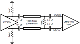
    OSCin is LVPECL, interconnection as follows:

    Based on the VCXO datasheet, its kvco is 7.5kHz/V, you may need to recalculate the loop filter. BTW, why choose this PLL-based VCXO? Non PLL-based 100MHz VCXO is very common in the market.

  • Hi, thanks.

    I readed datasheet 9.1.2 section named "Driving CLKin and OSCin Inputs", but in this chapter i see just recomendations for CLK inputs, so i was not sure in 100%, that this refers OSC inputs too.
    But after change VCXO-OSCin (LMK) connection like in Figure 22 (Your second graphics) LMK locks both PLLs, so im really happy, and gratefull for Your patience and help.
    But story not ends, because OSCin (and of course CLKouts) frequency is 100MHz - 390Hz, this shift depends on temperature. Now i got almost stable PCB temp. Aut if i will let her to heat, the frequency shift groves (for about 1000Hz).
    This shift causes bigger shift on LMXs outputs: for example 1070MHz -4kHz, where 1070MHz is target. I know VCXO has some temperature stability, but with LMK i expect more accurracy. What depends on?
    I will try to decerase PLL1 loop bandwith, but i will gratefully for Your suggestions.

    I will change kvco too. I don't know why PLL based VCXO was choosen.
    Skippnig that availability fact, this shouldn't cause problems in design launch and accuracy? I ask just for sure.

    We probably want use this chips in further project, but we need to now to be sure that they allow as to achaive good frequency accuracy and stability.

  • Hi There,

    If both PLL1 and PLL2 are locked, that means they are all locked to the FPGA CLKin clock. Their frequency accuracy (in ppm) is therefore equal to the frequency of the FPGA clock. You said VCXO frequency is 100MHz - 390Hz, check the FPGA clock frequency, it should be same. If they are not the same, probably the VCXO Vtune input pin is leakage. You can increase PLL1 charge pump current to resolve this problem.

    The problem with PLL-based VCXO is it has higher phase noise vs regular VCXO. 

  • Hi,

    I forgot about LTC6952 which is between FPGA and LMK. Its work as distributor, and jitter cleaner. But i checked drift of clocks when PCB temperature changes about 25 deg C. And probably reference clock for FPGA (XO, 30ppm) is source of unstability - its 200MHz, and drifts about 840Hz (4,2ppm). This drift its proportionally transferred to FPGA->LTC->LMK->LMX, with exception LTC6952 which reduce it about 2-3x. So i will try to change XO to TXCO with stability 2,5ppm. 

    On another board i have LMX2581 working with just VCXO ASG-P-V-A-100.000MHz as reference (OSCin) and i'm wondering why its VCXO has frequency miss about 10kHz when VC pin is unconnected. This is about outside the tolerance limits resulting from the documentation. My conclusion is that crystal oscillators in this design has to bad stability for RF solutions. 

    I thought for a moment about capacitors (pF) added to standard XOs, but while for standard XOs the documentation specifies the load capacity and the articles describe the use of these capacitors, for this type of oscillators the load capacity is usually not specified and their use is not described anywhere, but I guess they are not applicable due to differences in oscillator designs. Can You confirm it?

  • Hi Ks,

    for below statement, what oscillator you are in doubt about? XO or VCXO?

     for this type of oscillators the load capacity is usually not specified and their use is not described anywhere, but I guess they are not applicable due to differences in oscillator designs

  • Hi,

    I think about both of them, but as i thought and as You wrote - capacitors are not used for them.

    Changing XO to TCXO with 2.5ppm stability as clock for FPGA changes temperature drifts on LMX's outputs from 4,5kHz (max) to 280Hz (max) - that's enaught :)

    But for trhird LMX which has OSCin singnal directly from XO(VCXO with floating VC pin) this TXCO isn't suitable, because has LVDS output, so i think voltage swing will be not enaught to trigger LMX OSCin pin.

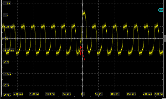
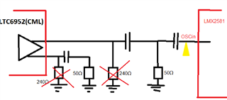
    So i wired OSCin to LTC6952 output (CML), by third types of matching/termination circuit. As last i used suggested by You before for LMK->LMX connection, and i cant achaive any sinal on outputs, but as i observed, two times i get R/4 signal on LD pin - i'm mainly focused on achaiving this signal, it it will be proper, i will try to achaive output signal. Two times after enabling device i see 6,25MHz signal on LD pin so it was proper, but now i can't achaive it. Below i show OSCin voltage and circut. Voltage looks proper but on LD pin just after writing config i get just some signal 625kHz, about 400kHz, and after that about 4MHz one by one by several ms, and after that signal goes low. Can You suggest something? 

     
    The same voltage with hanged time base, red arrow shows config writing moment. It can be scope "quirk", but on low time base signal looks stable.

  • Hi KS,

    The LTC has CML output, you should not put the shunt resistors at its output.

    You cannot floating the Vc pin of a VCXO, if there is no PLL to control the VCXO, we should put a fixed voltage, usually Vcc/2 to the Vc pin. 

  • Hi, 

    I thought that LMX OSCin internal circut was broken, because i still can't get R/4 singal on LD pin, so i replaced LMX, and removed 240R shunts, and it starts work. But after several on-off cycles problems back, and as i see OSCin voltage swing was out off spec (too high) so i added couple (10) ohms series to reduce swing and it starts work again. I properly thought that to high voltage swing on OSCin pin will be ignored by LMX? It's looks like.

    I thougt that VC pin should be pulled to half supply voltage (usually as You say), but when it was pulled to full supply voltage frequency should me nominal+(or-)pulling range, but was more different than pulling range, and too much unstable for our solution so i think with vcc/2 voltage, frequency off set will be still unacceptable high (+divider resistor tolerance influence), and stability will be of course still unacceptable, so i resigned from him.

    So, thank You so much Noel Fung :) Im really nice suprised by Your current support and day after day answers. Not every manufacturer provides such support. Maybe i will ask something new if something will uexpectable explodes and stops work - i can't promise ;)

  • Hi KS, 

    Thank you for using TI products, feel free to post when you have application issues.