This thread has been locked.

If you have a related question, please click the "Ask a related question" button in the top right corner. The newly created question will be automatically linked to this question.

NE555: NE555

Part Number: NE555
Other Parts Discussed in Thread: TLC555, TINA-TI

Hi TI team,

I am working on buck converter where I am using NE555 timer IC to generate PWM for mosfet gate drive. I want to design a output voltage feedback (closed loop) based buck converter to control my output voltage at every load condition.

From NE555 timer IC, I am able to generate PWM (as a A-stable multi-vibrator) but I want to control my PWM width with the help of Feedback circuit. Kindly suggest how can vary pulse width w.r.to output voltage feedback circuit.

Thanks

  • Hi Munesh,

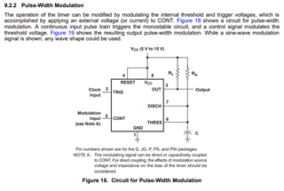
    The recommended PWM circuit for NE555 is the monostable configuration. This configuration allows for voltage-controlled PWM by applying a control voltage at the CONT pin. See section 9.2.2 from the NE555 datasheet below.

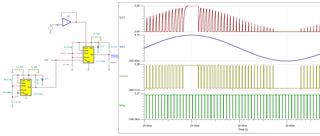
    I've also attached a TINA-TI simulation file showing the voltage-controlled PWM function using the TLC555 model.

    PWM_NE555.TSC

    Be aware that 555 timers configured as gate drivers are susceptible to inductive kickback from the transistor. A common failure mode is that inductive kickback can drive the output voltage above the rail, which can cause damage to the device in an over-voltage condition. In order to mitigate damage to the 555 timer in this situation, it is recommended to design in TVS (transient voltage suppression) diodes on the output of the 555 timer to the VCC supply rail.

    Regards,

    Zach

  • Hi Zach,

    Thanks for immediate response and your suggestion. In that buck converter application, I don't have such any trigger input to operate 555 as monostable. As I mentioned I need to vary PWM by buck output voltage (to stablize my output). Can I change anything in the ckt to get desired result. 

  • Hi Munesh,

    In the astable configuration the frequency and duty cycle are determined by the charging/discharging of the RC network. Attempting to apply a control voltage to change the duty cycle will also result in a changing frequency. If you require a constant frequency output with voltage-controlled duty cycle, the monostable configuration is the best option.

    For your trigger source, you may use another 555 timer in the astable configuration to generate a clocking pulse. See updated schematic and TINA file.

    PWM_555_Mono_Astable.TSC

    Regards,

    Zach

  • Hi Zach,

    Above TINA reference ckt is very helpful. I understood, trigger source can be adjusted (on time & off time). 

    In my application, VG1 (Control input at 2nd 555) is not analog input. It's a feedback voltage which is in DC voltage form (5V or other DC reference voltage using voltage divider) from buck converter output side. So I have to vary on time (duty cycle 37%) accordingly with constant switching frequency (650Khz).

    Kindly give more insight about it.

    Thanks

    Munesh Tripathi

  • Hi Munesh,

    I'm sure we could design a voltage feedback control scheme as you described. However, your switching frequency of 650kHz is much too fast for the NE555 timer which has a minimum monostable pulse width of 10μs (see section 8.3.1 of NE555 datasheet).

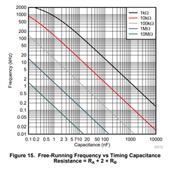
    It may be possible to achieve this using the TLC555 instead which can operate with a minimum pulse width of 1μs. However, in practice it is difficult to achieve accurate results above 100kHz due to propagation delays, component tolerance, board parasitics, on-state resistance, and process variation. Figure 15 from the TLC555 datasheet (below) shows significant curvature (non-linear) behavior at frequencies above 100kHz.

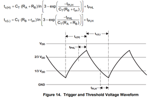
    Operating at frequencies above 100kHz greatly complicates the timing and duty cycle analysis as many additional factors must be considered, including propagation delay times which can vary up to 30% over process. See figure 14 from TLC555 datasheet.

    I believe we could come up with an accurate design for your proposed circuit if we can limit the switching frequency to ~100kHz.

    If this is not an acceptable tradeoff, Texas Instruments offers integrated solutions for DC/DC switching regulators including buck converters. This will allow you to greatly simplify your design and will likely be very cost-effective while also saving space on your PCB.

    I briefly looked through the available devices and saw many buck converters with switching frequencies in the 100s of kHz range and even up to a few MHz. You can browse these integrated solutions at the following link:

    https://www.ti.com/power-management/non-isolated-dc-dc-switching-regulators/step-down-buck/overview.html

    If you require additional support in your regulator design or for specific part recommendations feel free to post a question to the Power Management forum.

    Best Regards,

    Zach