A related question is a question created from another question. When the related question is created, it will be automatically linked to the original question.
If you have a related question, please click the "Ask a related question" button in the top right corner. The newly created question will be automatically linked to this question.
Thanks. I just checked LMC567 and got a question about the pinout.
On the page 3 of the ds, pin 5 is marked as T-cap and pin 6 is marked as T-res, however in the typical application block diagram and the layout diagram on page 10 and page 12 they seem to be reversed(pin 5 is T-res and pin 6 is T-cap). Also I compared with LM567's pin setup and layout, and it seems like they got almost the same layout, while LM567 has it's pin 5 marked as T-res and pin 6 as T-cap.
Could you help check if the pinout on LMC567 ds is correct?
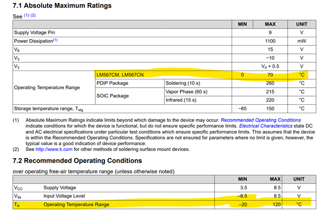
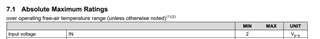
Also, I in 7.1 the device's maximum rating is 2Vp-p minimum for input voltage, could you elaborate what does this mean?(Is the minus mark missing here?)