Part Number: LMK04832
Hi:
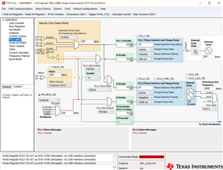
In my design, I use an external 200M crystal oscillator connected to CLK_in0 as the reference clock input for LMK04832. The OSCout outputs 200M as the working clock for the FPGA, ensuring that the FPGA can operate after power-on and configuring the LMK04832. I will use DCLK out2 as the 100M ADC_clk output, SDCLK out3 as the SYSREF output, and DCLK out8, DCLK out10, DCLK out12, SDCLK out9, SDCLK out11 as the 100M FPGA DDR4 controller input reference clocks. I will use the 0 delay mode to ensure all output clocks have a fixed phase relationship. I have installed TICS Pro and TI PLLatinum Sim, I am learning to use.
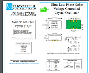
- If my crystal oscillator performance is good, do I definitely need to use an external VCXO? Do I need to use CVPD-952 as the 200M VCXO? The image shows available frequencies that do not include 200M,does this mean I cannot use it?
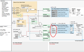
- I'm not very clear on which pins the feedback circuit of the zero delay mode needs to use( datasheet show that "zero-delay feedback may performed with an internal feedback from CLKout6, CLKout8, SYSREF, or with an external feedback loop into the FBCLKin port as selected by the FB_MUX." If choose an internal feedback ,I need not to make any other external pin connections for the 0 delay mode? if so, I'd like config DCLKout6 as internal feedback ), and how to use PLLatinum Sim determine the capacitance and resistance values of the loop filter. Can you provide a schematic diagram for a dual loop 0 delay mode reference design using an external VCXO? If an external VCXO is not necessary, could you provide a schematic diagram for a single loop 0 delay mode?