This thread has been locked.

If you have a related question, please click the "Ask a related question" button in the top right corner. The newly created question will be automatically linked to this question.

LMK04832: Multi System Sync Approach Review

Part Number: LMK04832
Other Parts Discussed in Thread: LMK5B33216

Hi Team, 

Kindly help to review the approach, please suggest if we missed anything.

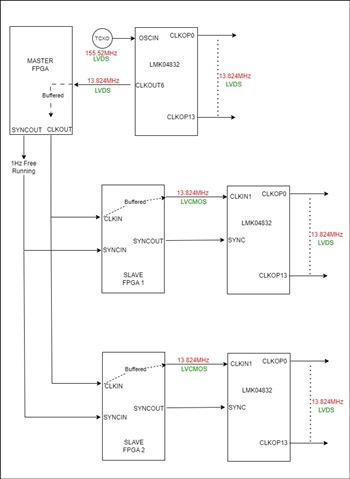
Target: We are using single PLL mode, and wish to synchronize the slave systems to the master system without any clock breakout.


Approach:

For the master device, the LMK04832 will generate the O/P clocks with the external TCXO (155.52MHz) connected to the OSCin Pin. Internal FB from CLKOUT6 is used for Cascaded 0-delay.
One of the clock outputs (13.824MHz) is fed back to the master FPGA. This clock and 1Hz Sync Pulse is transferred (buffered) from the master FPGA to the slave FPGAs. 

Slave FPGA receives the clock (13.824Mhz) and uses this for the LMK Clock Input connected to the CLKIN1 pin. The slave FPGA synchronizes the SYNC OUT pulse with the SYNCIN which is fed to the LMK SYNC to synchronize the CLKOUTs with the master system.

The slave LMKs are synced with the master system once the power is on.

  • Arjeet,

    I will confirm this setup today.

    Regards,
    Will

  • Ok Will,

    I believe the SYNC pulse may not be needed to sync the slave device with the master, as it will be synced with the input clock(from master). Please help to confirm this point too.

  • Arjeet,

    Sorry for the delay.  I will try to get an answer to you by tomorrow.

    Regards,

    Will

  • Apologies for the delay Arijeet, several people went out of office for US holiday and we didn't hand off your question properly.

    When you say "synchronize the slave systems to the master system", does that mean they're the same frequency and arbitrary phase? Or the same frequency and the same phase? The former is very straightforward, the latter is more complicated. I'm assuming the latter (same frequency and same phase), since otherwise you could just use a buffer and you would not need any SYNC behavior.

    Getting the slave clocks precisely phase-aligned to the master is more complicated than just running in zero-delay mode... there's latency between CLKOUT6 at the master LMK pins and CLKin1 at the slave pins, and that latency may be different between different slave devices if the total travel distance or the buffer propagation delay mismatch is large. If you could guarantee a SYNC pulse arrives at each LMK at the same time, this could reset all the output dividers to within one VCO cycle (presumably 2488.32MHz, or about 400ps). There's no mechanism in the LMK for device clocks to correct skew beyond one-half of a VCO period, and half-cycle correction would be open-loop - you'd have to know you need to do it from experimental measurement, and the conditions under which it's required may change over temperature. Maybe your FPGA has adjustable delays on the buffer, which could be used to tune out the last element of variation.

    If ±200ps phase alignment between devices is acceptable, I think the scheme above could be made to work; even nominal ±100ps is feasible if you can do some rough characterization to know when a device needs its half-step tuning engaged. If you have some capability to delay the clock to each slave device through the master FPGA output buffer, you could get much closer to exact phase alignment, but the characterization work likely increases and may differ over process at the FPGA.

    As far as eliminating the SYNC pulse, it could be done if the config is designed correctly:

    • Put the slave devices in zero-delay mode
    • Set all the digital delays to the same value as the zero-delay feedback
    • Ensure the R-divider is equal to 1 (or you would end up with potentially multiple phases after sync)
    • Provide a SYNC pulse at any time, even over software - exact timing does not matter since zero-delay will servo all outputs to alignment with the input

    Whether or not you use a SYNC pulse, you will incur some phase noise penalties with this approach - between the FPGA buffering the output and the lower phase detector frequency at the slave LMKs, the offsets below about 1MHz will likely see a significant phase noise increase (3 to 5 dB). The only way to avoid this would be distributing the original 155.52MHz reference everywhere, which avoids cascading multiple PLLs.

  • Hi Sir,

    We agree with the points you discussed.

    Since our systems are placed some distance apart distributing a 155.52 MHz clock wouldn't be a feasible approach for us.
    We are planning to use this chipset on a data acquisition system and clock output breakout option because the sync pulse is not acceptable in the end application.


    We are planning that our individual systems will work with their own free-running OSC (TCXO) & we will distribute a low freq clock (sync clock) let's say 1KHz/2KHz. The output clocks will be phase-aligned to this low freq. ref clock.

    Request you to suggest your views on this or any other approach. Any similar TI solutions would be helpful for us. 

  • If you distribute a low-frequency clock, the PLL which receives it should have a loop bandwidth around 10x-100x lower, for stability reasons. This is infeasible with PLL2, since you'd need something like 10-100Hz loop bandwidth and it's unlikely you can make PLL2 stable at such a low loop bandwidth. Additionally, since you're suggesting that higher frequencies are infeasible due to distance, you'd necessarily be reducing your PLL2 phase detector frequency and hindering your phase noise performance.

    A separate problem with the described approach is that giving each system its own free-running oscillator will result in frequency mismatch between the systems. To get these frequency-locked, they'd need to be running at the same frequency, or else they'd need to be feedback-controllable such that you could lock them inside another PLL.

    There's a way to do this with LMK04832, but it requires:

    • Using a VCTCXO or a VCXO instead of a free-running TCXO as a VCO in PLL1
    • Locking PLL1 to a low-frequency sync clock
      • Needs to be higher than 300kHz due to maximum SYSREF divider size limitations
      • Needs to be an integer divisor of desired output clock
    • Setting each LMK04832 SYSREF divider to run at the same frequency as the input reference clock
      • This restricts the SYSREF divider, so if you were planning to use it this may not be an option
    • Putting the device in nested zero-delay mode and retiming any SYNC event to the SYSREF divider edge
    • If output edges across all LMK04832 must be simultaneous, the low-frequency SYNC clock phase to each LMK must be aligned to make that possible

    In this scheme, we utilize a zero-delay configuration with the SYSREF divider in the feedback loop, since the SYSREF divider can also be used as a retimer for SYNC events. If the reference frequency and the SYSREF divider frequency are made equal, there's only one possible system phase for the SYSREF divider across every LMK device. By retiming the SYNC event to the SYSREF divider, we can guarantee the SYNC event occurs only at a specific phase alignment with the reference edge. So as long as we can make the reference clock arrive at each PLL simultaneously, no timing-critical SYNC is required to get frequency and phase alignment across multiple systems.

    ---

    As an alternative, maybe you can consider something like LMK5B33216. This device has DPLLs that can handle very low reference clocks, so sending a low-frequency signal at 1-2kHz would be acceptable. The DPLLs then act as extra control loops which can correct a cascaded fractional PLL locked to a free-running oscillator. You can also handle reference clock propagation delay correction directly at the DPLL by simply entering a correction word to the DPLL's TDC phase (TDC is analogous to phase detector), without needing to precisely align the reference inputs.

    With one of these devices, my only caveat is that you don't want to use a 155.52MHz TCXO, or any free-running oscillator that would produce a strictly integer divisor relationship between the VCO frequency and the XO port. Since the DPLL is correcting the frequency error of a free-running fractional PLL, error between the sync clock and the free-running XO port in an exact integer PLL configuration will produce very large integer boundary spurs. Something like a 100MHz TCXO would be a better choice, since there's no integer relationship between the expected VCO frequency and the reference input.

    The setup with the device would look like:

    • Configure DPLL2 to receive the low-frequency 1-2kHz sync clock; leave DPLL1/DPLL3 disabled
    • Provide a non-integer-related frequency to the XO port (e.g. 100MHz) and configure APLL2 to produce the desired outputs; leave APLL1/APLL3 disabled
    • Configure the device in zero-delay mode, to ensure there is always an output clock edge at every reference edge
    • Compensate for any known delay across multiple systems by supplying a correction word to the DPLL, which can be adjusted dynamically (with smooth phase slewing) at runtime if needed
  • Hi Sir,

    I am bit confused to configure ticspro for LMK5B33216.

    Can you please help me with the ticspro configuration file for our requirement.

    Output Clock 13.824MHz

    Sync/ref Clock 1KHz/2KHz.

  • Arijeet,

    Yes, we will configure a ticspro configuration for your requirements next week. 

    Regards,

    Will

  • Hi Arijeet,

    I'm working on the TICSPRO configuration for this.Please clarify:

    • Are you able to provide 10-kHz sync clocks instead of 1-kHz? For Zero-Delay Mode, we recommend using input frequencies of at least 8 kHz to ensure fast lock times.

    Regards,

    Jennifer

  • Sorry, Jennifer we can have max sync of 2Khz

  • Arijeet,

    Do you plan to switch between multiple 1-2 kHz inputs? The problem is that there is a risk of the DPLL railing off for low frequencies with ZDM; this is more a concern with 1-PPS but it could be 1 kHz. I would need to test.

    If you only plan on having one reference input, then I don't have a concern and I can work on configuration. Please confirm if that is the case.

    Regards,

    Jennifer

  • Hi Jennifer, 
    We will use 2KHz as reference input. We will not switch between multiple inputs

  • Hi Arijeet,

    Thank you for confirming. I can work on a configuration for a 2 kHz input with ZDM on LMK5B33216. This will take me about a week to configure.

    What is the output frequency plan? Are all outputs 13.824 MHz?

    Regards,

    Jennifer

  • Ok. I will work on the config and reach back next week.

    Regards,

    Jennifer

  • Hi Arijeet,

    Please try with this configuration: LMK5B33216_XO=48MHz_REF=2kHz_OUTs=13.824MHz, ZDM.tcs

    ZDM feedback output to DPLL2 is OUT0. All outputs are set to 13.824 MHz and sourced from APLL2. Both IN0 and IN1 are configured for a 2 kHz frequency.

    Regards,

    Jennifer