This thread has been locked.

If you have a related question, please click the "Ask a related question" button in the top right corner. The newly created question will be automatically linked to this question.

TLC555: Output Accuracy/Tolerance of TLC555 in Astable mode

Part Number: TLC555

Hello,

I want to use TLC555 as Astable multivibrator to generate 100KHz square wave with 50% duty cycle. I was using TI calculator in which the propagation delays were included to estimate the output frequency tolerance. I would like to improve the tolerance of output frequency by choosing NPO/C0G capacitor with 5% toleranace but i am not sure how can I calculate the improved toelrance with C0G capacitor since the tool only uses predefined capacitor with 10% tolerance. If i want to use the formulas given in the datasheet there the propagation delays were not included. Could you please let me know how i can calculate/estimate the tolerance of output frequency for 100KHZ square wave with 50% duty cycle operated with Vcc=5V and 3.3V. 

Also the tool  throws an error when i dont select diode option. It says ''the resistor values are too small, please reduce the capacitor'' can you explain the reason behind this ?

Do you have any alternate cost effective solution for this requirement ?

  • Hi Manoj,

    This E2E FAQ page is a very useful reference for designing a-stable 555 timer circuits:  https://e2e.ti.com/support/clock-timing-group/clock-and-timing/f/clock-timing-forum/879112/faq-how-do-i-design-a-stable-timer-oscillator-circuits-using-lmc555-tlc555-lm555-na555-ne555-sa555-or-se555 

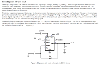
    On this page, you can find the following design to achieve 50% duty cycle using a single R and C component connected to the output and thresh/trig pins. The calculator tool requires the use of a diode to achieve the 50% duty cycle as you've discovered, however for the configuration shown, the diode is not required.

    You only require the diode for duty cycles less than 50% and this diode adds its own non-linearities as well. As you are operating at 50% duty cycle, this configuration is preferred to reduce complexity as you will already face the non-linearities associated with operating at higher frequencies.

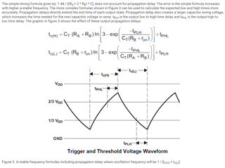
    The FAQ page recommends to account for the propagation delays according to the equations shown below. However, an engineer recently has measured the propagation delays to be ~215ns for both TPHL and TPLH. It is worth noting that these measured values are slightly different than the ones shown in the calculator tool. The values can also vary up to 30%. As these delays are approximately equal, in this configuration they can affectively cancel out resulting in the 50% duty cycle. As for your timing requirements, your error is likely to be dominated by component tolerance and board parasitics, not the propagation delays.

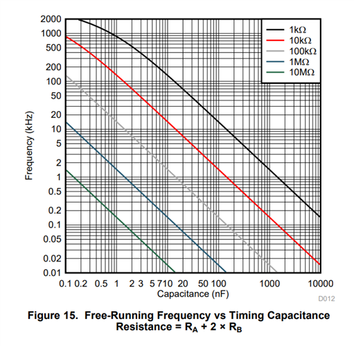
    In figure 15 below, you can see that there is significant curvature (non-linear) behavior at frequencies above 100kHz and the timing capacitor needs to be small for high frequencies. For this reason the tolerance of the capacitor must be well controlled and board parasitic capacitance must be accounted for. My recommendation is to use an LCR meter to measure the timing capacitor at the frequency of interest and also measure the board parasitic capacitance with the TLC555 removed from the board. This is because the parasitic capacitance will present in parallel to your selected capacitor value, resulting in the two capacitances to be added together which is the effective total capacitance CT. 

    My recommendation is to use the CT value to calculate your oscillation frequency, based on the equation: fosc = 0.721 / (Rc * CT). In addition you should account for the tolerances of components stated from the manufacturer. The timing capacitor is critical and should be film or COG/NPO. The tolerance of the capacitor will be given as 5% in some cases but it is important to measure at the frequency of interest as well to get an accurate value to plug in.

    There are some general best practice guidelines to follow for minimizing parasitic capacitance in the layout of the PCB.

    1. Increasing space between adjacent traces
    2. Cutting out power and ground planes above and below critical traces
    3. Minimizing component to component trace lengths. Shorter traces will have less capacitance due to capacitance per unit length.
    4. Minimizing use of Vias on critical traces.

    /resized-image/__size/800x500/__key/communityserver-discussions-components-files/48/3730.pastedimage1627592177092v2.png

    Regards,

    Zach

  • Hello Zach,

    Thanks for the response. This will certainly help !

    I am more interested in the frequency than the duty cycle. I understand that from the simple 50% duty cycle circuit, major contributions for the output frequency tolerance are R & C. I would like to know are they are any other parameters that i need to consider to estimate the output frequency tolerance ? does parasitic capacitance have any impact ? aslo, I can see in the datasheet the output high voltage information(as shown below) is not complete at full range, dooes it have any impact on the frequency ? I believe variation in threshold voltages have impact on propagation delays, does it have any impact ?

    Best Regards,

    Manoj

  • Hi Manoj,

    The three major error contributions to the frequency are the R and C component tolerance, the parasitic capacitance, and the non-linearity in the capacitance vs frequency curve (figure 15).

    The parasitic capacitance on your PCB can be measured and accounted for to reduce the error. This is the purpose of the CT term, which is the combination of the timing capacitor value and the measured parasitic capacitance.

    At the ~50% duty cycle and 100kHz, assuming the propagation delays are equal at ~215ns. The total timing error from both prop delays is 430ns which is a 4.3% error on the total time period of 10μs. You can target a slightly faster frequency to account for this timing delay.

    Subtle differences in the output high voltage should not significantly effect the timing, as the thresh pin only needs to charge to 2/3 of the supply voltage. As the Trig and Thresh pin are tied together, I don't believe variation in threshold voltage will cause a significant error.

    Regards,

    Zach