This thread has been locked.

If you have a related question, please click the "Ask a related question" button in the top right corner. The newly created question will be automatically linked to this question.

LMK04821: SPI read/write issue

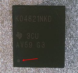
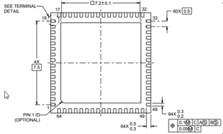
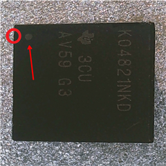
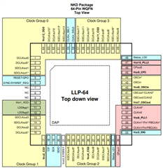
Part Number: LMK04821


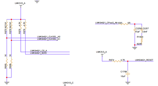
The chip is powered normally at 3.3V.SPI communication fail. There are only resistors between the FPGA and LMK04821, without any other components.

The LMK04821 is controlled by the FPGA, CSn cannot be pulled high. Changing the terminating resistor on CSn to 1K and reducing the distance to the LMK04821 to 1cm did not resolve the issue. FPGA and LMK04821 share the common ground.Measurements show:

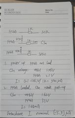
1. Upon system power-up without FPGA loading,the pin state of the FPGA is weak pull-up.Measuring the voltage across the  resistor, the voltage on the LMK04821 side is 1.56V, and on the FPGA side is 2.10V, so the input current of the CSn pin is 540uA.
2.While the FPGA is loaded and the SPI interface remains in its default state without sending data, driving CSn pin to a high level leads to the voltage on the LMK04821 side is 1.62V and the FPGA side  is 3.30V, the input current of the CSn pin is 1.68mA.
3. Under the second testing condition, multiple attempts were made to reset the LMK04821 chip via the Reset pin, while monitoring the CSn signal line on the LMK04821 side. However, nothing changed. According to the  datasheet regarding the CSn pin current, CSn can only be an input interface, with a maximum current of ±5uA. However, the actual measurement differs from the datasheet by several hundred times, indicating an abnormal power state for CSn.

Given that LMK04821 only needs stable 3.3V power and consistent high or low levels on the reset pin for proper operation, Is there any possibility that the above error state may occur,  what is the best way to rectify the problem?

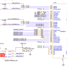
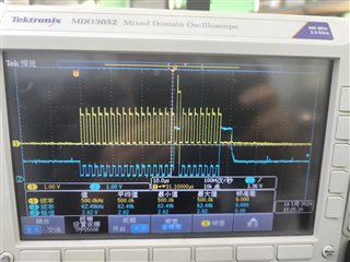
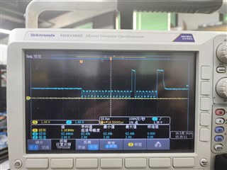
plus,in normal operation(terminating resistor 22ohm,SDIO pull-up 4.7K to 3.3V),sck high voltage is only 2V.SDIO cannot be held low.

  • Hello,

    I will get back to you tomorrow.

    Regards,

    Will

  • Hi, Will

       Please reply asap.It's kind of an emergency

  • Hi,

    Have you been able to replicate this issue on multiple devices or done any A-B-A swap testing?  

    Regards,

    Will

  • Hi,Will

    ALL the devices' wave form act the same. SPI write/read fail.

  • Hi ,any update for this question review? 

  • Good day , would you like to share the comments on this? Look forward to your reply today.

  • Hello Ben,

    It seems that there's something wrong on your hardware that's causing this issues. I'm also confused with the waveforms provided.

    1. Why do you have the 4.7kΩ to pull up? If you look at the LMK04832-SEPEVM which has the MCU (MSP430) included in the schematic, there are not pull or pull down resistors populated on the board. Also, bringing this up cause it seems like mainly a resistor setup issue between teh bus lines of the LMK04821 and the FPGA.

    2. Why are you sinking so much current in the CSn pin? This would only be true if the device is powered down or broken?

    3. What do the different waveforms represent on your scope captures?

    4. Are you following the correct timing requirements as explained on p. 25? For instance, are you leaving the CS pin high before starting to read/write, etc.

    4. I would recommend also talking to the FPGA team to understand the data they are sending and ensure the lines are being setup correctly (this ties a bit with point 1 as well).

    Hope this helps!

    Good luck,

    Andrea

  • Hi, Andrea

    1.  4.7k pull-up is recommended in the datasheet. As SPI  in 3-wire mode, SDIO as an output(open-drain mode),pull up resistor is needed.

       In fact, we've tried SDIO push-pull mode before(remove the 4.7k),it also didn't work.

    2. I'm also confused what causes this issue. CS pin is pull-up 4.7K to 3.3V. I wonder if there is a suggested pull-up resistor value.

    We've tried a whole new board(cut off all components' power supply except FPGA&LMK04821) which is never powered on before, it also didn't work.

    3.I'm sorry I didn't describe it clearly before. In the 1st picture,

      1(the yellow waveform ):SPI SCLK  As shown in the picture , SPI SCLK high voltage is only 2V. We've checked the power supply, it's correct.

    Besides, the waveform in the FPGA side is correct when we remove the 22ohm resistor. Once connecting to LMK04821, problem occurs.

      2(the blue waveform): SDIO DATA    As shown in the picture , SDIO cannot be held low.

    It's data waveform in the 2nd picture, and SCLK waveform in the 3rd picture.

    4.Timing requirements is met. Only when writing/reading operation ,CS is held low.

    As illustrated, we intend to write 0x000(adress),0x80(data) ,which is 000 0000000000000 10000000.

    But SDIO cannot be held low to gnd,it may cause the writing error.

  • The SPI SCLK, SDIO, and CS pins are all nominally high-impedance. You are seeing results that suggest an implausibly high current for typical operation. This suggests the device is damaged, not fully started up, or otherwise electrically connected in a way that is causing a large amount of current to sink into what are normally high-impedance input pins.

    • Check the power pins and make sure power is actually being applied to all pins. There are 12 of them, and all 12 of them need to be 3.3V.
    • Check the schematic or layout to confirm there are no unexpected shorts on the nets.
    • Check the orientation of the device on the board. I have at least once seen bewildering effects caused by the device being rotated 90°.
    • Check the reset pin voltage and make sure the pin isn't oscillating around mid-range of the supply voltage.
    • Remove the 22Ω resistor from the board again and check the pin voltages at SCLK, SDIO, and CS pins on the LMK04821 side. Are there bias voltages other than 3.3V or GND? This would be highly unexpected.
    • Check that 3-wire SPI isn't causing a bus conflict that could lead to damage. If you attempt to do a readback transaction (first bit of address is high) and the FPGA interface is still actively driving the SDIO line after 16 bits of data, it's possible you are creating a bus conflict where the FPGA driver is pushing current into the open-drain stage of the SDIO pin. Does your configuration use 3-wire SPI? If it doesn't, are you sure that you set SPI_3WIRE_DIS=1 in the register map during initialization before conducting any readback? If you can't, can you instead make sure to use open-drain signaling from the FPGA on the SDIO pin as well?
  • Hi,Derek

    I'd like to know if the dot stands for pin1. It works when we rotate the device 90°. But the dot does not stand for pin1

  • According to our topside marking metadata in the packaging and assembly database, the dot is the pin1 marking - the package engravings are rotated clockwise 90° relative to the pin 1 marking dot. This dot should also line up underneath the package with a chamfered corner on the thermal DAP, but I see that this is marked "optional" on the datasheet, so it may not be present.

    To be clear: pin 1 should be in the location circled below. I have rotated the package image to orient the pin 1 marking in the upper-left corner, such that it matches the top-down view provided in the pinout diagram in the datasheet (to the right of the rotated image below).

    Please double confirm, you are absolutely certain, that the pin 1 location does not correspond to the dot or the chamfered DAP (on device underside) as described in my images above?

    If pin 1 really is in the wrong place on your devices, there are significant additional steps we need to take to determine whether this is a genuine unit, and if so the potential scope of impact.