Part Number: LMX2572LP
Other Parts Discussed in Thread: , LMX2581, LMX2572
How about an update on PLLatinum Sim.
I am running a simulation with LMX2572LP.
I ran the PLL simulation and saved the results (Fig 1).
Then I load the results and input 280MHz again and the loop bandwidth and phase margin values change (Fig 2).
Which result is correct?
I downloaded the PLLatinum Sim from the website (Fig 3), but the situation remains the same.
I would like to know the correct result as I will start PCB design in the near future.
Regards,
Akihiko Yokouchi
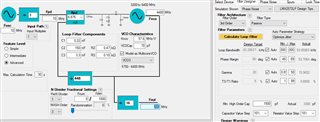 Fig 1
Fig 1
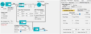 Fig 2
Fig 2
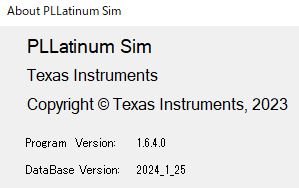 Fig 3
Fig 3


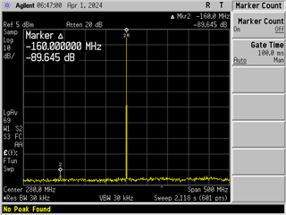
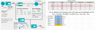 fig1
fig1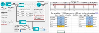 fig2
fig2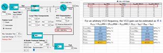 fig3
fig3