This thread has been locked.

If you have a related question, please click the "Ask a related question" button in the top right corner. The newly created question will be automatically linked to this question.

CDCEL913: How to Configured using I2C

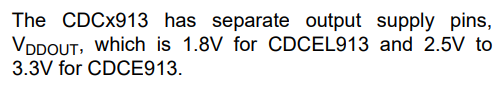
Part Number: CDCEL913
Other Parts Discussed in Thread: AM5728, , CDCE913

Hello,

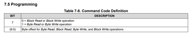
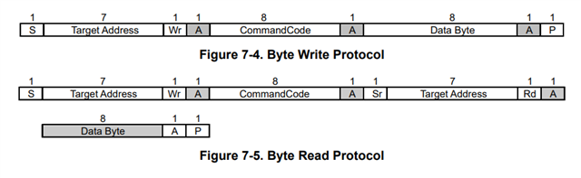
In our Custom Board (AM5728 ) we are using cdcel913 chip for clock generation and it is interface using I2C.

I'm using VxWorks OS , I want to configure the this but I unable to find any source.

please tell me how can we configure this.

And is there any differences between cdcel913 and cdc3913.

Best Regards.

Hanmant

  • Hanmant,

    The differences between the CDCE913 and the CDCEL913 are only the supply voltage:

    We do not have standalone drivers for this device. We offer the TI Clock Pro software for configuration with an evaluation module, or for creating configurations that can be exported to a file. We strongly recommend using the software for creating a configuration file, which can then be used by your system.

    Thanks,
    Kadeem

  • Thanks for clarification .

    I have configured chip .

    My input frequency is 12Mhz and expecting output like 40.96MHz on Y1 and Y2 output but i'm getting on 572KHz on Y1 and no output on Y2

    please see below configuration:


    vxbI2cWriteCdce(UINT8 *)0x05,0x83,sizeof((UINT8 *)0x05));//Data_Bytes , Command offset bytes ,Length

    vxbI2cWriteCdce((UINT8 *)0x28,0x85,sizeof((UINT8 *)0x28));


    vxbI2cWriteCdce((UINT8 *)0x1D,0x94,sizeof((UINT8 *)0x1D));

    vxbI2cWriteCdce(0x00,0x96,sizeof(0x00));

    vxbI2cWriteCdce(0x00,0x97,sizeof(0x00));

    vxbI2cWriteCdce((UINT8 *)0xF0,0x98,sizeof((UINT8 *)0xF0));


    vxbI2cWriteCdce(0x00,0x99,sizeof(0x00));

    vxbI2cWriteCdce((UINT8 *)0x7A,0x9A,sizeof((UINT8 *)0x7A));

    vxbI2cWriteCdce((UINT8 *)0x23,0x9B,sizeof((UINT8 *)0x23));

    vxbI2cWriteCdce((UINT8 *)0xF0,0x9C,sizeof((UINT8 *)0xF0));

    vxbI2cWriteCdce((UINT8 *)0x00,0x9D,sizeof((UINT8 *)0x00));

    vxbI2cWriteCdce((UINT8 *)0x7A,0x9E,sizeof((UINT8 *)0x7A));

    vxbI2cWriteCdce(pCDCEDev,(UINT8 *)0x20,(UINT8)0x6F,sizeof((UINT8 *)0x20));

  • Hanmant,

    Please see the below register configuration file for creating a 40.96MHz output on Y1 and Y2 using a 12MHz XTAL. If this is an LVCMOS clock, then R1[3:2] should be 0b10 instead of 0b00.

    CDCE913_12MHz_in_40p96MHz_out.TXT

    Thanks,
    Kadeem

  • Hi Kadeem ,

    Thank for your support .

    Can you please tell me how to calculate Command code offset Bytes ,in 0 to 7,7th bit is byte read /write right? and another 0 to 6 bit how to calculate? 

  • Hanmant,

    Not sure what you mean here. The bits provided in the above file are simply the bitwise contents of each register.

    Bit 7 in the command code is for whether or not a byte or block operation is being performed. Bytes 6:0 are the register to read/write. See below for the full transaction:

    Thanks,
    Kadeem

  • Hello Kadeem,

    still I do have confusion related this Bytes 6:0 are the register to read/write.

    Can you give me example of registers.

  • Hello,

    The Command Code bits 6:0 indicate what register you are reading or writing to for that I2C transaction. So say you wanted to write to decimal Register 15. The Command Code [6:0] would be 0001111

    Best,

    Cris