Other Parts Discussed in Thread: LMK5B33216
Hello TI team,
I am trying to evaluate LMK05318B for one our designs and following is the requirement:
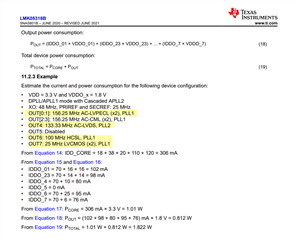
IN: 40MHz XTAL, 40MHz recovered clock
OUT: 156.25MHz(HCSL), 122.88MHz(LVCMOS), 40MHz(HCSL) and 10MHz(LVCMOS)
Is this combination possible with single chip LMK05318B?
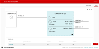
Trying out in your webench clock tree architect tool, as expected the chip is generating two arbitrary frequencies required using APLL1 and 2. Alongside, 10MHz is also given which is shown is from VCO1. For 40MHz, the tool is recommending to go with another chip cascaded to it's 10MHz output. So my query is:
- How is the chip able to get 10MHz alongside the 156.25MHz while it is not an integer divided value from 156.25MHz? (it is only 10MHz and not any other frequency seen possible)
- One of the datasheet example cases (page 76) show the generation of 100MHz and 25MHz along with two aribitary frequencies. From what configuration are these numbers arrived?