This thread has been locked.

If you have a related question, please click the "Ask a related question" button in the top right corner. The newly created question will be automatically linked to this question.

LMX2592: LMX2592 Losing Lock after Tuning

Part Number: LMX2592


Hi,

We are seeing an issue with the LMX2592 PLL. When we change the output frequency from 2.451GHz to 2.551GHz, and then back to 2.451GHz, the PLL loses lock. We initially thought this was an issue with writing to REG30, and to the VTUNE_ADJ register, which got added in a newer version of the datasheet. We removed any writes to the VTUNE_ADJ bits in REG30, and the problem seemed to dissapear, but we are now discovering an intermittent fault on a board with this again. Our code originally did no writes to the VTUNE_ADJ bits, but since this was recently added to the datasheet, this got added in to our interface code.

We are wondering, if A : does VTUNE_ADJ need to be set on temperature dependent scenarios?

and B : does VTUNE_ADJ need to be written in a specific order, i.e do other registers need to be set up beforehand?

Many Thanks,

James

  • Hi James, 
    A quick check does seem to indicate this. Seems the register was added to allow functionality a bit below -40 degC. 

    https://e2e.ti.com/support/clock-timing-group/clock-and-timing/f/clock-timing-forum/1131480/lmx2592-register-settings

    In regards to programming - yes. 

    Also, registers must be programmed in descending order. 

    Regards, 

    Vicente 

  • Hi TI

    Please can you help us?

    We find that when we tune your LMX2592 from one frequency to another then back again to the original, it looses lock. The output signal really is at the wrong frequency, it's not just the lock detetct function that's failing. It fails like this over a number of pairs of frequencies and it appears sensitive to the board temperature. Above about 60degC it fails in this manner. I have performed some thermal calculations and I'm very confident that we are nowhere near the maximum recommended junction temperature, in fact we are at a junction temperature of less than 70degC.

    We find that when we force CP_ICOARSE to be value 3, that is x2.5, it fixes the problem. Of course this is against the recommended advice in the datasheet and on this forum. What do you recommend we do to fix the problem?

    I attach three register map dumps for two example frequencies. The file with "bad" in the name is the failing condition. Note the fOSCin frequency is changed between the frequencies pairs, this is done to try to avoid fractional N spurs (IBS).

    Thanks in advance.

    JP

    --------------------
    LMX2592 PLL Good Registers for 6762.5MHz with fOSCin = 166.66666666MHz
    --------------------
    R0_CONTROL                     = 0x2210    
    R1_CAL_CLK_DIV                 = 0x808     
    R2                             = 0x500     
    R4_ACAL_CMP_DLY                = 0x1943    
    R7                             = 0x28B2    
    R8_VCO_OVR                     = 0x1084    
    R9_OSC_2X_REF_EN               = 0x302     
    R10_MULT                       = 0x10D8    
    R11_PLL_R                      = 0x18      
    R12_PLL_R_PRE                  = 0x7001    
    R13_CP_EN_PFD_CTL              = 0x4000    
    R14_CHARGE_PUMP_CURRENTS       = 0xD6A     
    R19_VCO_IDAC                   = 0x965     
    R20_ACAL_VCO_IDAC_STRT         = 0x12C     
    R22_VCO_CAPCTRL                = 0x2300    
    R23_VCO_SEL                    = 0x8842    
    R24                            = 0x509     
    R25                            = 0x0       
    R28                            = 0x2924    
    R29                            = 0x84      
    R30_VCO_DOUBLE_MASH_DITHER     = 0x34      
    R31_VCO_CHDIV_DIST             = 0x401     
    R32                            = 0x210A    
    R33                            = 0x2A0A    
    R34_CHANNEL_DIVIDER_ENABLE     = 0xC3CA    
    R35_CHANNEL_DIVIDER_SEGMENTS   = 0x19      
    R36_CHANNEL_DIVIDER            = 0xF11     
    R37_PLL_N_PRE                  = 0x4000    
    R38_PLL_N                      = 0x28      
    R39_PFD_DELAY                  = 0x8204    
    R40_PLL_DENOMINATOR_MSB        = 0x3B9A    
    R41_PLL_DENOMINATOR_LSB        = 0xCA01    
    R42_MASH_SEED_MSB              = 0x0       
    R43_MASH_SEED_LSB              = 0x0       
    R44_PLL_NUMERATOR_MSB          = 0x1122    
    R45_PLL_NUMERATOR_LSB          = 0xE6E0    
    R46                            = 0x1FA3    
    R47_OUTA_MUX_OUTB_PWR          = 0x8CF     
    R48_OUTB_MUX                   = 0x3FC     
    R59_MUXOUT_HIGHDRIVE           = 0x0       
    R61_LD_TYPE                    = 0x1       
    R62                            = 0x0       
    R64_CAL_AMP_FREQ               = 0xAF      
    R68_VTUNE_LD                   = 0x4E8     
    
    --------------------
    LMX2592 PLL Good Registers for 6862.5MHz with fOSCin = 133.333333333MHz
    --------------------
    R0_CONTROL                     = 0x2210    
    R1_CAL_CLK_DIV                 = 0x809     
    R2                             = 0x500     
    R4_ACAL_CMP_DLY                = 0x1943    
    R7                             = 0x28B2    
    R8_VCO_OVR                     = 0x1084    
    R9_OSC_2X_REF_EN               = 0x302     
    R10_MULT                       = 0x10D8    
    R11_PLL_R                      = 0x18      
    R12_PLL_R_PRE                  = 0x7003    
    R13_CP_EN_PFD_CTL              = 0x4000    
    R14_CHARGE_PUMP_CURRENTS       = 0xC61     
    R19_VCO_IDAC                   = 0x965     
    R20_ACAL_VCO_IDAC_STRT         = 0x12C     
    R22_VCO_CAPCTRL                = 0x2300    
    R23_VCO_SEL                    = 0x8842    
    R24                            = 0x509     
    R25                            = 0x0       
    R28                            = 0x2924    
    R29                            = 0x84      
    R30_VCO_DOUBLE_MASH_DITHER     = 0x34      
    R31_VCO_CHDIV_DIST             = 0x401     
    R32                            = 0x210A    
    R33                            = 0x2A0A    
    R34_CHANNEL_DIVIDER_ENABLE     = 0xC3CA    
    R35_CHANNEL_DIVIDER_SEGMENTS   = 0x19      
    R36_CHANNEL_DIVIDER            = 0xF11     
    R37_PLL_N_PRE                  = 0x4000    
    R38_PLL_N                      = 0x32      
    R39_PFD_DELAY                  = 0x8204    
    R40_PLL_DENOMINATOR_MSB        = 0x3B9A    
    R41_PLL_DENOMINATOR_LSB        = 0xCA01    
    R42_MASH_SEED_MSB              = 0x0       
    R43_MASH_SEED_LSB              = 0x0       
    R44_PLL_NUMERATOR_MSB          = 0x2BC5    
    R45_PLL_NUMERATOR_LSB          = 0xAC59    
    R46                            = 0x1FA3    
    R47_OUTA_MUX_OUTB_PWR          = 0x8CF     
    R48_OUTB_MUX                   = 0x3FC     
    R59_MUXOUT_HIGHDRIVE           = 0x0       
    R61_LD_TYPE                    = 0x1       
    R62                            = 0x0       
    R64_CAL_AMP_FREQ               = 0xAF      
    R68_VTUNE_LD                   = 0x4E8     
    
    --------------------
    LMX2592 PLL Bad Registers for 6762.5MHz with fOSCin = 166.66666666MHz
    --------------------
    R0_CONTROL                     = 0x2210    
    R1_CAL_CLK_DIV                 = 0x808     
    R2                             = 0x500     
    R4_ACAL_CMP_DLY                = 0x1943    
    R7                             = 0x28B2    
    R8_VCO_OVR                     = 0x1084    
    R9_OSC_2X_REF_EN               = 0x302     
    R10_MULT                       = 0x10D8    
    R11_PLL_R                      = 0x18      
    R12_PLL_R_PRE                  = 0x7001    
    R13_CP_EN_PFD_CTL              = 0x4000    
    R14_CHARGE_PUMP_CURRENTS       = 0xD6A     
    R19_VCO_IDAC                   = 0x965     
    R20_ACAL_VCO_IDAC_STRT         = 0x12C     
    R22_VCO_CAPCTRL                = 0x2300    
    R23_VCO_SEL                    = 0x8842    
    R24                            = 0x509     
    R25                            = 0x0       
    R28                            = 0x2924    
    R29                            = 0x84      
    R30_VCO_DOUBLE_MASH_DITHER     = 0x34      
    R31_VCO_CHDIV_DIST             = 0x401     
    R32                            = 0x210A    
    R33                            = 0x2A0A    
    R34_CHANNEL_DIVIDER_ENABLE     = 0xC3CA    
    R35_CHANNEL_DIVIDER_SEGMENTS   = 0x19      
    R36_CHANNEL_DIVIDER            = 0xF11     
    R37_PLL_N_PRE                  = 0x4000    
    R38_PLL_N                      = 0x28      
    R39_PFD_DELAY                  = 0x8204    
    R40_PLL_DENOMINATOR_MSB        = 0x3B9A    
    R41_PLL_DENOMINATOR_LSB        = 0xCA01    
    R42_MASH_SEED_MSB              = 0x0       
    R43_MASH_SEED_LSB              = 0x0       
    R44_PLL_NUMERATOR_MSB          = 0x1122    
    R45_PLL_NUMERATOR_LSB          = 0xE6E0    
    R46                            = 0x1FA3    
    R47_OUTA_MUX_OUTB_PWR          = 0x8CF     
    R48_OUTB_MUX                   = 0x3FC     
    R59_MUXOUT_HIGHDRIVE           = 0x0       
    R61_LD_TYPE                    = 0x1       
    R62                            = 0x0       
    R64_CAL_AMP_FREQ               = 0xAF      
    R68_VTUNE_LD                   = 0xE8      
    

  • Hi John, 

    We find that when we tune your LMX2592 from one frequency to another then back again to the original, it looses lock. The output signal really is at the wrong frequency, it's not just the lock detetct function that's failing. It fails like this over a number of pairs of frequencies and it appears sensitive to the board temperature. Above about 60degC it fails in this manner. I have performed some thermal calculations and I'm very confident that we are nowhere near the maximum recommended junction temperature, in fact we are at a junction temperature of less than 70degC.

    Okay, sounds like you have confirmed the device is in fact locked using the a signal analyzer to determine carrier frequency is in fact incorrect. As reported in the thread I attached in my previous response - many times by setting CP_ICOARSE larger than 1.5x  the device LD would report being unlocked but in fact it is still locked. 

    Can you provide a snippet of your schematic? I am interested in seeing your loop filter design. 

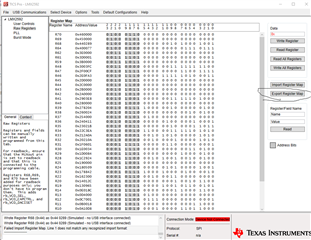
    I also cannot import your register map to TICSpro GUI. 
    Can you upload registers dumps once more using TICSpro "Export Register Map" button"? 

    Or better yet, can you attach a .tcs configuration file instead? 

    Regards, 

    Vicente 

  • Loop Filter image attached.

  • Actually those register dumps were made by our software and are nothing to do with TICS, however your request for a TICS compatible dump prompted me to reverse engineer back into TICS. Doing so highlighted a possible problem, we are not obeying the FCAL_HPFD_ADJ requirements. We'll try to implement the proper configuration and try again.

    Thanks for your help.

    JP

  • Hi John,

    Right, FCAL_HPFD_ADJ was not configured to match fpd, this is one of the issues in your configuration. The biggest problem with your configuration, however, is you did not set FCAL_EN=1. That means, when you change the VCO frequency, there is no VCO calibration, this is probably the main reason why you did not get it locked. 

  • Thank you very much I hadn't spotted that. Actually though, I thought that bit self reset? If it doesn't self reset and I need the calibration to run,  then it always needs to be set?

  • Hi Vicente

    You suggest "Also, registers must be programmed in descending order." This does not seem to agree with the datasheet section 7.5.2? Which is correct?

    Thanks

    JP

  • Hi John, 
    FCAL_EN is not self clearing here. 

    Only reset is self clearing in DS. 

    If you're trying to change VCO frequencies you will need to have this bit set otherwise like Noel stated you will no trigger a VCO calibration in the process. 

    Upon initial startup you will need to program the device in descending order. Once the part is initialized and setup properly, you can follow section 7.5.2 to program only the registers you need to edit to change frequencies. 

    Regards, 

    Vicente 

  • Hi Vicente

    What order do we use if we are changing things like the charge pump currents, the VCO doubler, the R dividers and frequency?

  • Hi John, 
    If you implement any changes that require a VCO calibration I would still program registers in descending order. 

    Regards, 

    Vicente