This thread has been locked.

If you have a related question, please click the "Ask a related question" button in the top right corner. The newly created question will be automatically linked to this question.

LMK00804B: VIL and VIH of the LVCMOS_CLK pin do not satisfy the characteristics of datasheet

Guru 12185 points
Part Number: LMK00804B

Hi,

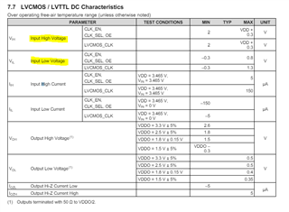
It appears that VIL and VIH of the LVCMOS_CLK pin do not satisfy the characteristics. Without considering the transmission delay of Tpd = 1 to 2.2 ns, the output of all 4 channels seemed to change at approximately 0.45 V and approximately 2.9 V.

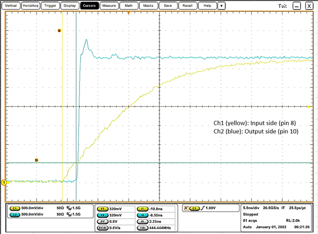
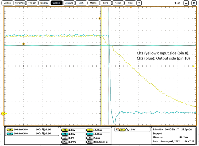
We have verified this using official TI samples and commercially purchased products, and the results are similar and there appears to be no lot dependence.

Is it possible to get any comments?

Thanks,

Conor

  • Conor,

    Could you clarify which spec is being violated and what your issue is, it is unclear to me?

    Regards,

    Will

  • Hi Will,

    VIH is over 2V, but if you look at the first waveform, you can see that the high output is around 0.5V. The maximum VIL is 1.3V, but if you look at the second waveform, you can see that the low output is around 2.8V.

    Is my understanding wrong?

    Thanks,

    Conor

  • Conor,

    I think I understand what you are saying.  The specs VIH and VOL are not references to the switching point of the input, only the acceptable input low and high voltage levels.  So your waveform actually does look in spec.  Your VIL (input low voltage) is ~0V which is > -.3 and < 1.3.  Your VIH (input high voltage) is ~3.3V which is >2 and is most likely > VDD + .3.  

    Are you seeing duty cycle problems?  Let me know if you have any more questions.

    Regards,

    Will

  • Hi Will,

    The specs VIH and VOL are not references to the switching point of the input, only the acceptable input low and high voltage levels. 

    I interpreted it as follows from the description in the data sheet.
    ① When Vin=-0.3~1.3V, Vout=Low is guaranteed
    ② When Vin=2.0~3.6V, Vout=High is guaranteed
    ③ Switching threshold is between 1.3 and 2.0V

    In your answer, it seems that the output is not guaranteed to be low even when Vin = -0.3 to 1.3V. Is there any information about switching thresholds?

    Thanks,

    Conor

  • Hello Conor,

    This seems to relate to a really similar question I've been dealing with in E2E as well (here is the link but since it's internal, I'm not sure if you'll have access to it).

    Either way even though this is a LVCMOS buffer (takes in an LVCMOS signal and outputs an LVCMOS signal), the input driver is not designed as your typical CMOS driver. Instead, it functions as a differential driver. We labeled V_IH and V_IL as described in the data sheet since you need to meet those requirements to obtain a 50% duty cycle. Hope this helps.

    Best,

    Andrea

  • Hi Andrea,

    Sorry, I don't fully understand.
    My understanding is as follows:

    With LVCMOS, when it is above Vdd x 50%, it is judged to be H level, and when it is below, it is judged to be L level. Specifically, when VDD = 3.3V, the threshold is 1.65V (VIL/VIH).

    What does VIL/VIH indicate in the datasheet? Also, I couldn't see the E2E link, so if you don't mind, would you be able to reformat it so that it can be viewed from outside and send it to me?

    Thanks,

    Conor

  • Conor,

    Unfortunately, I can't reformat the E2E link since it's an internal E2E and cannot be shared with non-TI people.

    V_IH and V_IL basically determine the limits your signal needs to swing around to ensure the part "sees" that input. Think of it as the signal needs to swing outside those values to make sure it's big enough to be "seen" by the 804B.

    Based on the picture above, the signal needs to swing outside the V_IH and V_IL values, basically in the direction of the arrows.

    However, the LMK00804B doesn't really follow this if 50% duty cycle is not required. Instead, the a swing of about 200mV needs to be achieved to see a square wave at the output.

    Best,

    Andrea

  • Hi Andrea,

    Thank you for your reply.

    V_IH and V_IL basically determine the limits your signal needs to swing around to ensure the part "sees" that input. Think of it as the signal needs to swing outside those values to make sure it's big enough to be "seen" by the 804B.

    VIH is the voltage that the input voltage is recognized as high when it exceeds this value, and VIL is the voltage that the input voltage is recognized as low when it is below this value. I think your answer is the same definition as VIH/VIL that is commonly used.

    My question, as stated in my first post, is about the timing of VOUT switching relative to VIN. In the capture in my first post, Vout switches from LOW to HIGH when VIN is about 0.4V, and from HIGH to LOW when Vin is about 2.9V. Where in the data sheet should I refer to for specifications regarding the timing of VOUT switching relative to VIN rising and VOUT switching relative to VIN falling?

    LMK00804B doesn't really follow this if 50% duty cycle is not required. Instead, the a swing of about 200mV needs to be achieved to see a square wave at the output.

    I didn't understand the above, so could you please explain it in more detail?

    Thanks,

    Conor

  • Hello Conor,

    My question, as stated in my first post, is about the timing of VOUT switching relative to VIN. In the capture in my first post, Vout switches from LOW to HIGH when VIN is about 0.4V, and from HIGH to LOW when Vin is about 2.9V. Where in the data sheet should I refer to for specifications regarding the timing of VOUT switching relative to VIN rising and VOUT switching relative to VIN falling?

    This behavior is correct/expected; however, those values are not in the data sheet, unfortunately. I'm planning to include them in the next data sheet revision. We tested the switching thresholds in lab and noticed the same behavior as you did.

    I didn't understand the above, so could you please explain it in more detail?

    Basically, if you do not meet the V_OH and V_IL, then you're signal is not guaranteed to have a 50% duty cycle.

    Best,

    Andrea