This thread has been locked.

If you have a related question, please click the "Ask a related question" button in the top right corner. The newly created question will be automatically linked to this question.

CDCE913: CDCE913PW

Part Number: CDCE913

Tool/software:

Hello,Team,

I have questions about CDCE913PW.
Are there any issue that output clk freqency is not lock such as freqency is keeping shift?
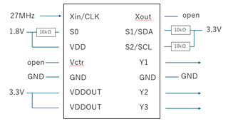
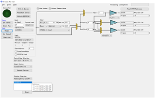
We use this device with below register setting.
<register setting>
0x00:81 /0x01:09 /0x02:B4 /0x03:09 /0x04:03 /0x05:50 /0x06:40 /0x07:0 /0x08:0 /0x09:0
0x0A:0 /0x0B:0 /0x0C:0 /0x0D:0 /0x0E:0 /0x0F:0 /0x10:0 /0x11:0 /0x12:0 /0x13:0 /0x14:0D
0x15:01 /0x16:0 /0x17:0 /0x18:C0 /0x19:04 /0x1A:82 /0x1B:07 /0x1C:C0 /0x1D:04 /0x1E:82 /0x1F:07

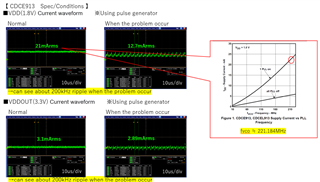
In rare cases, if you turn the power off and on again, Output frequency keeps shifting that is not desired.(but Y1Y2Y3 out put are in sync.)
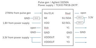
As you can see with above register setting ,We use Y1Y2Y3 output are the same frequency from the same div.
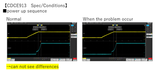
In the first place, Does the clock output even though the output is not stable when the power is turned on?
Normally, a stable clock is output after a while, but in rare cases(above case) it continues to be output without being stable.
We guess something wrong with PLL.

Thank you for your support

  • Hello,

    Does the output frequency get to the set frequency, then start to shift more over time? Also, how rare is the case?

    I will try to replicate this on our end tomorrow.

    Regards,

    Andrew

  • Hello,Team,

    This case,output frequency does not get to set frequency, all the time frequency keep shifting.
    And this occur approximately once in 100 times.
    As a supplement, inputclock is stable and you can see our circuit conditions by below figure.

    And the output clock is not stable when the power is turned on as a specification of this device?

    Thank you for your support

  • Hello,Team,

    Additional information.
    This case is that the clock input uses a clock generated by the FPGA rather than a crystal oscillator.
    At startup, the FPGA's output is initially fixed low and then starts outputting the clock.
    In this case, I am thinking that it may have occurred because the input was in a LOW period at the beginning.
    Therefore, are there any regulations regarding the time from when the device is powered on until the clock is input?
    Also, how does the output of this device behave when there is no input?

    The currently confirmed status is shown below.
    <From the device is powered on until the clock is input>
    ・INPUT:LOW → OUTPUT:HIGH fixed orLOW fixed or keep shifting.
    <After the clock is input>
    ・INPUT:27MHz → OUTPUT:24.576MHz(correct clock) or keep shifting

    Thank you for your support

  • Hello,

    We are testing the device and cannot recreate the error so far, although not with a FPGA. How fast are you power cycling the device? We will setup a test to verify it over time. Also, for the clock generation, can you check if the input is still correct from the FPGA when the drift occurs? The input timing requirements are in the table below:

    how does the output of this device behave when there is no input?

    When there is no input, the device will not have an output if the configuration is set to use the same input.

    are there any regulations regarding the time from when the device is powered on until the clock is input?

    There are no regulation for the chip itself, the input clock can be connected to the device before or after power on. 

    Regards,

    Andrew

  • Hello,

    Could you also provide a scope capture of the VDD and VDDOUT of the device during the defect, specifically for the rising edge. 

    Regards,

    Andrew

  • Hello,Team,

    Thank you for replying.


    We are testing the device and cannot recreate the error so far, although not with a FPGA. How fast are you power cycling the device? We will setup a test to verify it over time. Also, for the clock generation, can you check if the input is still correct from the FPGA when the drift occurs? The input timing requirements are in the table below
    →I repeatedly set the device ON with 30s and OFF 5s to cause this problem.
     I had checked the frequency, but I had not checked the rise time, fall time, or DUTY, so I will re-check and re-post.

    how does the output of this device behave when there is no input?
    When there is no input, the device will not have an output if the configuration is set to use the same input.
    →When the FPGA starts up, LOW is input to the Xin, but at that time, there are three cases in which the output is fixed at HIGH, fixed at LOW, and unstable, which seems to be different from the specifications.

    Could you also provide a scope capture of the VDD and VDDOUT of the device during the defect, specifically for the rising edge.
    →I will check again and repost.

    Thank you for your support

  • Hello,Team,
    Additional informations.

    This problem was reproduced by using a pulse generator instead of the FPGA as the clock input.
    The power supply uses a stabilized power supply to supply 3.3V/1.8V.
    The method is to supply the device with 3.3V/1.8V with a regulated power supply.
    Then, after 30 seconds, the pulse generator supplies clock at 27MHz (1.8V).
    If this problem does not occur, turn off the stabilized power supply and pulse generator output again and try the above method again.
    We was able to reproduce this in about 20 times, so please try repeating it 20 to 50 times.

    We also confirmed that the input waveform when the problem occurred met the timing requirements and was unchanged from normal case.
    We have not been able to confirm the VDD/VDDOUT waveforms, but we have reproduced it using the method above, so I assume that VDD/VDDOUT is not related to this problem.

    Thank you for your support

  • Above, I said 20 to 50 times, but it is currently difficult to reproduce the above number of times.
    Therefore, try repeating this for about an hour or more.
  • Hello,

    We have ran about 100 power cycle tests over an hour and did not see a drifting output. A few questions to hopefully identify the issue:

    • Are you switching the pulse generator on 30 seconds after turning on the power supply, then checking the measurement before powering off both the supply and pulse generator? We have a 1 second delay put in before measuring and powering off.
      • When the FPGA starts up, LOW is input to the Xin, but at that time, there are three cases in which the output is fixed at HIGH, fixed at LOW, and unstable, which seems to be different from the specifications.

      Is the LOW signal still a clock frequency input or a stable voltage? Without the input the output clock should not be outputting varying frequencies. What is the HIGH and LOW fixed values?

    • Is the current draw from the power supplies different during defect vs the stable output?

    For further support, like shipping the part to TI for additional testing if needed, can we move to email? You can reach me at a-lin@ti.com 

    Thanks,

    Andrew

  • Hello,Team,

    We have ran about 100 power cycle tests over an hour and did not see a drifting output. A few questions to hopefully identify the issue:
    Are you switching the pulse generator on 30 seconds after turning on the power supply, then checking the measurement before powering off both the supply and pulse generator? We have a 1 second delay put in before measuring and powering off.
    →The ON/OFF is also done manually, so I don't think it's a problem since it's not strictly a 30s thing.
    In the first place, are the register settings we showed correct?
    Are the register settings you are trying to reproduce the same as those we have shown?
    If they are not the same, please check with the one we have provided.
    If this register setting value is incorrect, please provide the correct one.

    When the FPGA starts up, LOW is input to the Xin, but at that time, there are three cases in which the output is fixed at HIGH, fixed at LOW, and unstable, which seems to be different from the specifications.
    Is the LOW signal still a clock frequency input or a stable voltage? Without the input the output clock should not be outputting varying frequencies. What is the HIGH and LOW fixed values?
    →The LOW signal is a stable voltage. Therefore, we are wondering why this device get the output. In your environment, how does it behave when no input is applied after the power is turned on?
    In the first place, in terms of specifications, if the input is not receiving the correct clock, what is the state of the output terminal? (LOW fixed, HIGH fixed, high impedance)

    Is the current draw from the power supplies different during defect vs the stable output?
    For further support, like shipping the part to TI for additional testing if needed, can we move to email? You can reach me at a-lin@ti.com
    →Currently, we are not able to reproduce it well and cannot measure the current value.
    However, we have confirmed and reproduced the problem on 5 devices.
    4 units use FPGA clock input, 1 unit uses pulse generator input.
    The measurement at the input of the pulse generator is as shown in the attached photo.

    Thank you for your support

  • Add.
    Since the same problem occurred on 5 units as i said above, we guess that it is not an individual defect.

  • Hello,Team,

    more additional information,

    We was able to confirm the VDD/VDDOUT waveform during the problem occur using a probe.
    Photos of the results are attached.
    Regarding the rising waveform, there is no difference between normal and problem occur conditions.
    Regarding the current value, VDD was 21 mArms when normal and 12.7 mArms when abnormal, confirming the difference.
    No big difference was observed in VDDOUT.
    However, ripples have been confirmed when both VDD/VDDOUT are abnormal.
    Additionally, we have confirmed that when an abnormality occurs, lowering VDD from 1.8V lowers the output frequency, and raising it from 1.8V increases the output frequency.
    In normal, the output frequency does not change even if the VDD voltage is changed during normal operation.

    The PLL is used at fvco=221.184MHz with the current register settings, and as shown in Figure 1 of the specifications, I think the current value during normal operation is appropriate.
    I have also attached the CLOCLPRO screen for setting this register for reference.

    Thank you for your support

  • Hello,

    Thank you for sending more information. The registers you first sent did not have output 2 and 3 enabled (Y2Y3_ST1), but the other settings are the same. Attached is the register map we used for testing, to match your configuration picture.

    For the output without an input clock, S0 high enables the output, which should be open if no clock input, however there is a 3-state output set if device power down.

    Also, are you using the CDCE913 EVM? The EVM is what we are verifying this on, but if you can send information or a schematic about the PCB board it may help identify the issue further. For now we are trying to get to the root cause of this, but it is difficult due to being unable to replicate the problem. 

    CDCE913Setup.TXT

    Regards,

    Andrew 

  • Hello,Team,

    Sorry, the circuit diagram I provided was incorrect.
    before: S0=0(pullUP), AFTER: S0=0(pulldown)

    We haven't tested it with EVM.
    As shown in the attached photo, the board using the pulse generator is mounted on a universal board.
    A schematic diagram and photos are attached.

    The difference between the register value you sent and my setting value was 0x07 and 0x15.
    Regarding 0x07, it is Unused address range, so why is 40 written?
    Regarding 0x15, could you create the circuit as shown in the attached diagram and set the register values ​​to the same values ​​as mine and check again to see if the problem occurs?

    Thank you for your support

  • Is the PCB you are using CDCE913PERF-EVM?

  • Hello,Team,

    In our environment, we input the clock from the pulse generator 30 seconds after turning on the power and check the waveform.
    If the problem does not occur, it has been found that turning off the power and pulse generator for 5 seconds, then turning on the power and repeating the above steps ,might help you to reproduce this occur.
    plese try it.

  • Hello,

    Please be patient with us because will be some delay on further testing. We are using the CDCE913PERF-EVM, the configuration file is generated directly from the ClocksPro output, you can try loading it into the software to see if the config is the same as well. It is odd that the register is different.

    Are you able to pull the S0 pin high (Enabled) instead of low (3-state) and see if it is ok? That may fix the issue, otherwise we will need more testing.

    Regards,

    Andrew

  • Are you able to pull the S0 pin high (Enabled) instead of low (3-state) and see if it is ok? That may fix the issue, otherwise we will need more testing.
    →With our register settings, I think Y2Y3 is enabled when S0=LOW.
    If I'm wrong, please let me know.

  • We have confirmed this with a universal board as described above.
    In other words, instead of rewriting the register settings and outputting them each time like EVM, we write the data to the device's ROM(EEPROM is permanently locked.) and confirm the reproduction with universal board.
    Could you please confirm whether the problem can be reproduced under the same with our conditions?

  • Hello,

    Understood, thank you for the setup information. The registers do seem correct for the outputs when S0 is pulled down. Will get back to you when more testing is complete.

    Regards,

    Andrew

  • Hello,

    We have confirmed the issue with the shift and error in the output with the same settings. To fix, please try inputting the reference CLK input before the power on VDD.

    Regards,

    Andrew

  • Hello,

    I'm glad you were able to confirm the issue.
    Then we have four questions.
    ①What is the environment in which you were able to confirm the issue?
    ②You say that you want me to try turning on CLK before turning on VDD to fix, although this is not written in the specifications, are there any problems that could cause the device to break?
    ③If it is correct to put CLK before VDD, are the sequence specifications written somewhere? Or is it an unexpected bug?
    ④What was the cause of this problem issue?

    Regards

  • Hello,

    There is no problem inputting the clock before the VDD. Can you confirm if the fix solved the issue you reported?

    To share more details it would be great if we can take this offline. Please contact me at a-lin@ti.com and I can pull in additional support.

    Regards,

    Andrew