This thread has been locked.

If you have a related question, please click the "Ask a related question" button in the top right corner. The newly created question will be automatically linked to this question.

CDCVF25084: 3.3V input during Power OFF

Part Number: CDCVF25084
Other Parts Discussed in Thread: SN74LVC1G34, CDCE6214,

Tool/software:

Dear Technical Support Team,

If a High level of +3.3V is input to CLKIN with the power off, is there a possibility of device failure?

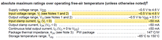
The VI in the datasheet does not seem to be specifically related to the VDD supply voltage.

The driver side is "SN74LVC1G34".

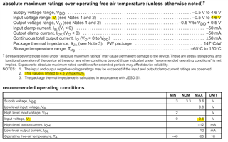
absolute maximum
VI : -0.5 V to 4.6 V

Recommended operating conditions
VI: 0V to 3.6V
Best Regards,

ttd

  • Hello,

    In many of our devices there is an ESD diode connecting the input pin to the VDD pin.  If a voltage is applied to the CLKIN the diode will allow current to flow and could lead to heat or high current flow through the VDD pin, both of which are bad for the part.  Because this is an older part from > 20 years ago, we do not have access to the design database and cannot check the internal structure to confirm whether or not this internal structure would be a problem.  So given this information, all we can do is not recommend that you drive CLKIN before the VDD pins.  

    Regards,

    Will

  • Hi Will,

    Thank you for your reply.

    In my understanding, when there is ESD diode between VIN and VDD, datasheet shows like VDD+0.5.

    However the datasheet shows only 4.6V(max).

    In general datasheet of TI(not only clock product), it means no ESD diode.  

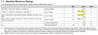
    For Example, CDCE6214 datasheet has absolute max of VIN: "VDD_REF +0.3", it means ESD diode.

    So I guess that CDCVF25084 doesn't have ESD and the withstand voltage to the positive side at the device's input (VIN) is probably covered by the process.

    I got your answer(we do not have access to the design database and cannot check the internal structure to confirm whether or not this internal structure would be a problem), however could you check it again? 

    Best Regards,

    ttd

  • Hello,

    I spoke with our Systems team and confirmed your assumption.  Because there is no Vdd reference in the input supply, it is safe to assume that there is no ESD diode and that powering CLKIN before VDD will work, as long as you stay below the input clamp current.  In regards to the design database, I confirmed we cannot check the internal structure.  

    Regards,

    Will

  • Hi Will,

    Thank you for your answer!

    I got that powering CLKIN before VDD will work. 

    Best Regards,

    ttd